Datasheet Summary
..
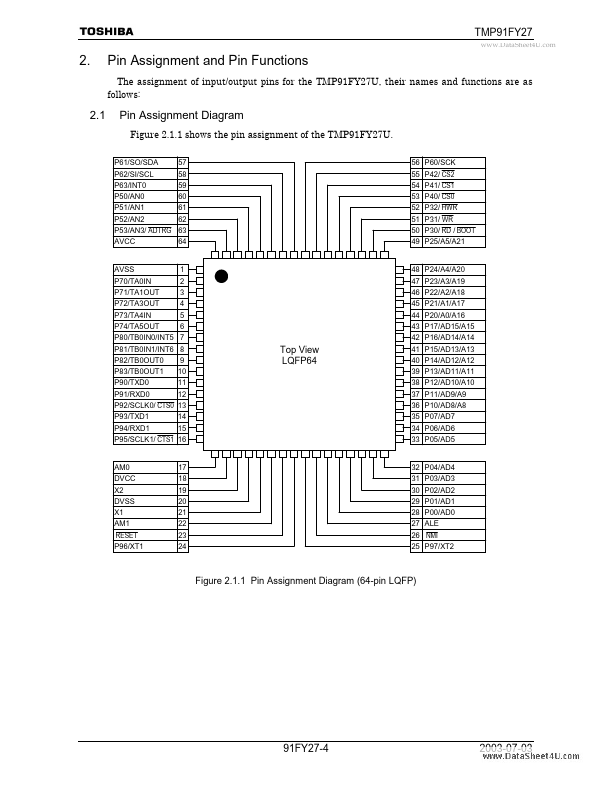
2.
Pin Assignment and Pin Functions
The assignment of input/output pins for the TMP91FY27U, their names and functions are as follows:
Pin Assignment Diagram
Figure 2.1.1 shows the pin assignment of the TMP91FY27U.
P61/SO/SDA P62/SI/SCL P63/INT0 P50/AN0 P51/AN1 P52/AN2 P53/AN3/ ADTRG AVCC 57 58 59 60 61 62 63 64 56 P60/SCK 55 54 53 52 51 50 49 P42/ CS2 P41/ CS1 P40/ CS0 P32/ HWR P31/ WR P30/ RD / BOOT P25/A5/A21
AVSS P70/TA0IN P71/TA1OUT P72/TA3OUT P73/TA4IN P74/TA5OUT P80/TB0IN0/INT5 P81/TB0IN1/INT6 P82/TB0OUT0 P83/TB0OUT1 P90/TXD0 P91/RXD0 P92/SCLK0/ CTS0 P93/TXD1 P94/RXD1 P95/SCLK1/ CTS1
1 2 3 4 5 6 7 8 9 10 11 12 13 14 15 16
48 P24/A4/A20 47 46...