JBT6K49-AS
JBT6K49-AS is Power supply IC manufactured by Toshiba.
..
TOSHIBA CMOS Digital Integrated Circuit Silicon Monolithic
Power supply IC for TFT LCD Panels
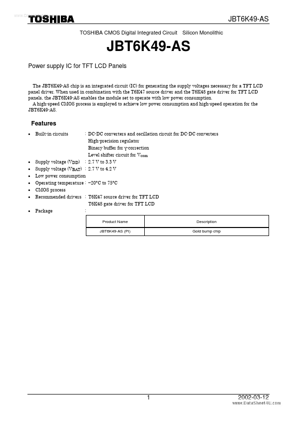
The JBT6K49-AS chip is an integrated circuit (IC) for generating the supply voltages necessary for a TFT LCD panel driver. When used in bination with the T6K47 source driver and the T6K48 gate driver for TFT LCD panels, the JBT6K49-AS enables the module set to operate with low power consumption. A high-speed CMOS process is employed to achieve low power consumption and high-speed operation for the JBT6K49-AS.
Features
- Built-in circuits : DC-DC converters and oscillation circuit for DC-DC converters High-precision regulator Binary buffer for γ-correction Level shifter circuit for V
- -
- -
- -
- Supply voltage (VDD) : 2.7 V to 3.3 V Supply voltage (VBAT) : 2.7 V to 4.2 V Low power consumption Operating temperature :
- 20°C to 75°C CMOS process Remended drivers : T6K47 source driver for TFT LCD T6K48 gate driver for TFT LCD Package :
Product Name JBT6K49-AS (PI) Description Gold bump chip
2002-03-12
..
Block Diagram
FSEL1 FSEL2 2 CA1+ CA1CA2+ CA2VDD /STB /RST /EXP
VSIN
VBAT
VSOUT1
CKSEL EXTCK
DC-DC Converter 1
Oscillation Circuit
CB1+ CB1CB2+ CB2CB3+ CB3CB4+ CB4CB5+ CB5VTOUT
Test Circuit REF Circuit DC-DC Converter 2
TEST SDA SCK FUSE-
- VREF VREFIN VSOUT2
VTIN CC1+ CC1GND (2) VBOUT
DC-DC Converter 3
Gamma Power Supply
VLC...


