Datasheet4U Logo Datasheet4U.com

T6K34 - Row Driver LSI

Features

  • LCD drive outputs: 168 common outputs Operating voltage: VDD = 1.8 V~3.3 V, VIN = 2.7 V~3.6 V (VDD ≤ VIN) LCD drive voltage: 28.8 V (max) Booster circuit: VIN × (.
  • 6) max Contrast control: 64 steps (max) Partial display function CMOS process Package: Bump chip (COF), TCP (tape carrier package) Low power consumption: ISS = 225 µA (typ. ) ……… Design target Conditions: VDD = VIN = 3.0 V, using ×5 booster, LCD non-leaded, Ta = 25°C, 1/168 d.

📥 Download Datasheet

Datasheet Details

Part number T6K34
Manufacturer Toshiba
File Size 75.46 KB
Description Row Driver LSI
Datasheet download datasheet T6K34 Datasheet

Full PDF Text Transcription (Reference)

The following content is an automatically extracted verbatim text from the original manufacturer datasheet and is provided for reference purposes only.

View original datasheet text
www.DataSheet4U.com T6K34 Preliminary TOSHIBA CMOS Digital Integrated Circuit Silicon Monolithic T6K34 Row Driver LSI for Dot Matrix Graphic LCD The TOSHIBA T6K34 is a row (common) driver for a small-to-medium-sized dot matrix graphic LCD. The T6K34 has 168 outputs for LCD driver signals (common). The T6K34 contains a power supply circuit with electronic volume enabling the LCD to be driven by a single power supply. Thus, in combination with a T6K33/S6B0021 (by Samsung) segment driver, the T6K34 can be used to implement a low-power LCD system without the need for a separate power supply IC. 
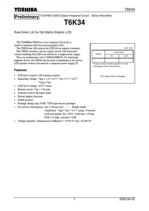
Unit: mm Lead Pitch T6K34 IN OUT Please contact Toshiba Agents for each Packaging Outline Dimensions. Features · · · · · · · · · LCD drive outputs: 168 common outputs Operating voltage: VDD = 1.
Published: |