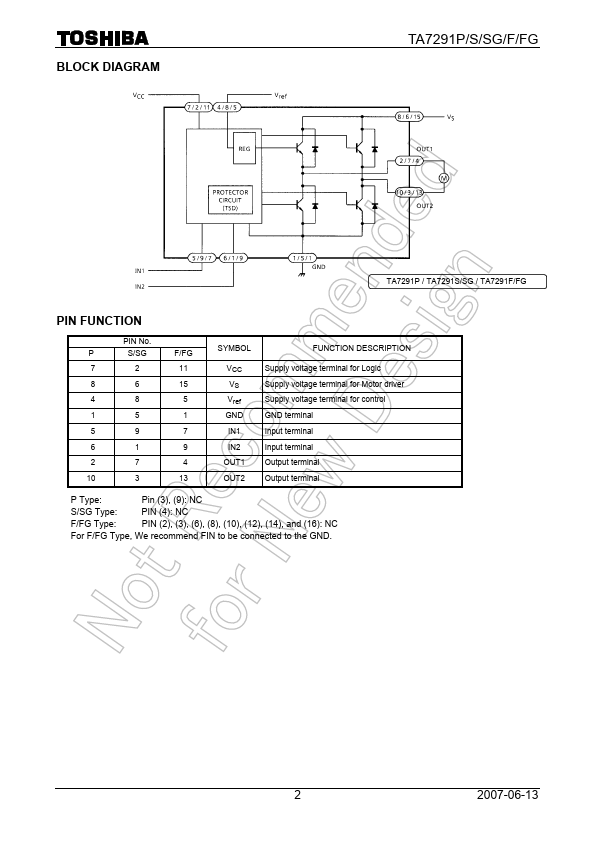
Datasheet4U Logo Datasheet4U.com

TA7291F - BRIDGE DRIVER

Description

7 2 11 VCC Supply voltage terminal for Logic 8 6 15 VS Supply voltage terminal for Motor driver 4 8 5 Vref Supply voltage terminal for control 1 5 1 GND GND terminal 5 9 7 IN1 Input terminal 6 1 9 IN2 Input terminal 2 7 4 OUT1 Output terminal 10 3 13 OUT2 Output

Features

  • z 4 modes available (CW / CCW / STOP / BRAKE) z Output current: P type 1.0 A (AVE. ) 2.0 A (PEAK) S/SG,/ F/FG type 0.4 A (AVE. ) 1.2 A (PEAK) z Wide range of operating voltage: VCC (opr. ) = 4.5~20 V VS (opr. ) = 0~20 V.
  • Please consider the internal loss (Vsat) to operate the IC though minimum VS is defined zero. Vref (opr. ) = 0~20 V z Build in thermal shutdown, over current protector and punch = through current restriction circuit. z Stand.
  • by mode available (STOP MODE) z Hysteresis for.

📥 Download Datasheet

Datasheet preview – TA7291F
Other Datasheets by Toshiba Semiconductor

Full PDF Text Transcription

Click to expand full text
TA7291P/S/SG/F/FG TOSHIBA BIPOLAR LINEAR INTEGRATED CIRCUIT SILICON MONOLITHIC TA7291P, TA7291S/SG, TA7291F/FG BRIDGE DRIVER The TA7291P / S/SG / F/FG are Bridge Driver with output voltage control. FEATURES z 4 modes available (CW / CCW / STOP / BRAKE) z Output current: P type 1.0 A (AVE.) 2.0 A (PEAK) S/SG,/ F/FG type 0.4 A (AVE.) 1.2 A (PEAK) z Wide range of operating voltage: VCC (opr.) = 4.5~20 V VS (opr.) = 0~20 V *Please consider the internal loss (Vsat) to operate the IC though minimum VS is defined zero. Vref (opr.) = 0~20 V z Build in thermal shutdown, over current protector and punch = through current restriction circuit. z Stand−by mode available (STOP MODE) z Hysteresis for all inputs. TA7291S/SG TA7291F/FG TA7291P, TA7291SG/FG: TA7291P Sn plated product including Pb.
Published: |