TA8207K
TA8207K is TOSHIBA Bipolar Linear Integrated Circuit Silicon Monolithic manufactured by Toshiba.
Features
- High power: POUT = 2.5W (typ.) (VCC = 9V, RL = 4Ω, f = 1k Hz, THD = 10%) POUT = 4.6W (typ.) (VCC = 12V, RL = 4Ω, f = 1k Hz, THD = 10%)
- -
- -
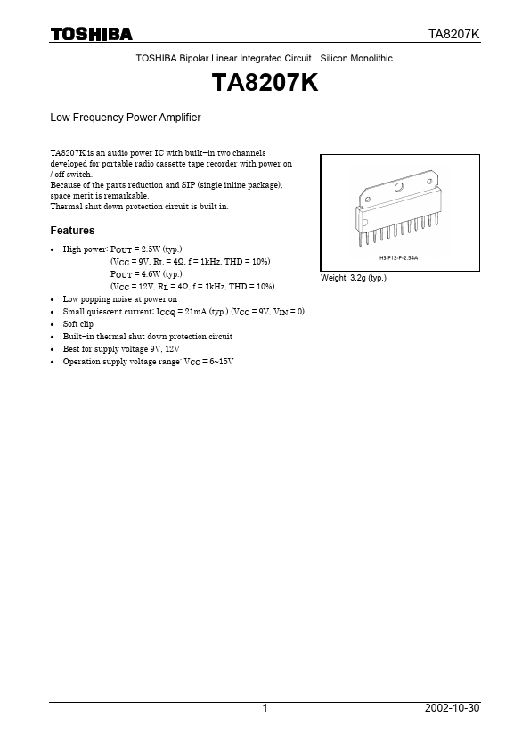
- - Low popping noise at power on Small quiescent current: ICCQ = 21m A (typ.) (VCC = 9V, VIN = 0) Soft clip Built- in thermal shut down protection circuit Best for supply voltage 9V, 12V Operation supply voltage range: VCC = 6~15V Weight: 3.2g (typ.)
2002-10-30
Maximum Ratings (Ta = 25°C)
Characteristic Supply voltage Output current (peak / CH) Power dissipation Operating temperature Storage temperature Symbol VCC IO (peak) PD Topr Tstg Rating 20 2.5 12.5 -20~75 -55~150 Unit V A W °C °C
Electrical Characteristics
(unless otherwise specified, VCC = 9V, RL = 4Ω, Rg = 600Ω, f = 1k Hz, Ta = 25°C, Rf = 120Ω)
Characteristic Quiescent current Output power Total harmonic distortion Symbol ICCQ POUT (1) POUT (2) THD GV (1) Voltage gain GV (2) Input resistance Output noise voltage Ripple rejection ratio Cross talk Input offset voltage Stand-by current RIN VNO R.R. C.T. V6, V7 IOFF
- -
- -
- -
- SW 1→off Test Circuit
- -
- -
- VIN = 0 THD = 10% THD = 10%, VCC = 12V POUT = 0.4W / ch Rf = 120Ω, VOUT = 0.775Vrms (0 d Bm) Rf = 0, VOUT = 0.775Vrms (0 d Bm)
- Rg = 10kΩ, BW = 20Hz~20k Hz Rg = 600Ω, fripple = 100Hz Rg = 600Ω, アンプ 1↔2, Vo = 0.775Vrms (0 d Bm), f = 1k Hz
- Test Condition Min.
- 2.0
- - 43
- -
- -
- -
- Typ. 21 2.5 4.6 0.2 45 56.5 30 0.3 52 50 30 1 Max. 45
- - 1.0 47 d B
- - 1.0
- - 60
- kΩ m Vrms d B d B m V µA Unit m A W %
Typical DC Voltage Of Each Terminal (VCC = 9V, Ta = 25°C)
Terminal no. DC voltage 1 8.7 2 4.5 3 VCC 4 5.0 5 0.7 6 0.03 7 0.03 8 0.7 9 GND 10 4.5 11 8.7 12 VCC
2002-10-30
Block Diagram / Test Circuit
(- 1): This IC can be used without coupling capacitor (CIN). If volume slide noise occured by input offset voltage is undesirable, it needs to use the capacitor (CIN). (- 2): The condenser between the (3) pin and the GND (C11) is for reducing pop noise when the power on / off switch (SW 1)...