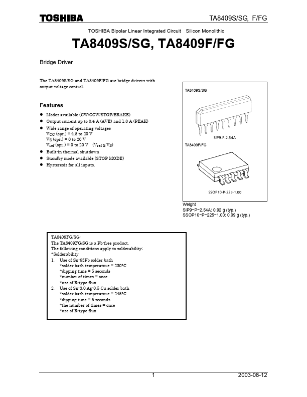
Description
TA8409F/FG
Pin No.1 2 3 4 5 6 7 8 9 10 Symbol IN2 VCC OUT2 NC GND NC VS OUT1 Vref IN1 Input terminal Supply voltage terminal for logic Output terminal Non-connection GND terminal Non-connection Supply voltage terminal for motor driver Output terminal Reference voltage terminal for control circuit.Input terminal Functional Description
Function
Input IN 1 0 1 0 1 IN 2 0 0 1 1 OUT1 ∞ H L L Output OUT2 ∞ L H L Mode MB STOP CW/CCW CCW/CW BRAK.
Features
- z Modes available (CW/CCW/STOP/BRAKE) z Output current up to 0.4 A (AVE) and 1.0 A (PEAK) z Wide range of operating voltages VCC (opr. ) = 4.5 to 20 V VS (opr. ) = 0 to 20 V Vref (opr. ) = 0 to 20 V (Vref ≤ VS) z Built-in thermal shutdown z Standby mode available (STOP MODE) z Hysteresis for all inputs. TA8409F/FG
Weight SIP9.
- P.
- 2.54A: 0.92 g (typ. ) SSOP10.
- P.
- 225.
- 1.00: 0.09 g (typ. )
TA8409FG/SG: The TA8409FG/SG is a Pb-free product. The following conditions.