
TA8483CP Description
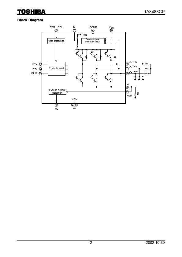
O Excess current detection signal output I Heat protection circuit selecting pin ― Mid-point voltage pin O Majority logical sum output (power output pin voltage detection circuit) ― GND O W -phase output pin O V -phase output pin O Current detection resistanse connecting pin O U -phase output pin I Supply voltage pin I U -phase input pin I V -phase input pin I W -phase input pin I Excess current detection input pin...
TA8483CP Key Features
- Built-in excess current detection function
- Built-in heat protection function
- The configuration of the output stage is shown in the chart to the right
- The PWM operation takes off-on control of the upper side transistor
- Be sure to set the schottky barrier diode outside, because the current flows to the lower-side diode when PWM is off
- The three-phase input receivs three-state impedance (high. low, high impedance) from the controller side
- When junction temperature Tj is Tj≥TSD (on) (overheat protection operation temperature)
- When TSD-SEL = "high", an automatic return mode takes place
- The voltage in current detection resistor RF outside VI pin is input to the VISD pin
- When VISD voltage rises above internal reference voltage VRF (≃ 0.5V), excess current detection circuit ISD bees "high"