Datasheet4U Logo Datasheet4U.com

TC74LVX74FN - DUAL D-TYPE FLIP FLOP WITH PRESET AND CLEAR

Download the TC74LVX74FN datasheet PDF. This datasheet also covers the TC74LVX74F variant, as both devices belong to the same dual d-type flip flop with preset and clear family and are provided as variant models within a single manufacturer datasheet.

Features

  • High-speed: fmax = 145 MHz (typ. ) (VCC = 3.3 V) Low power dissipation: ICC = 2 µA (max) (Ta = 25°C) Input voltage level: VIL = 0.8 V (max) (VCC = 3 V) VIH = 2.0 V (min) (VCC = 3 V) Power-down protection provided on all inputs Balanced propagation delays: tpLH ≈ tpHL Pin and function compatible with 74HC74 www. DataSheet4U. com TC74LVX74FT Weight SOP14-P-300-1.27: 0.18 g (typ. ) SOL14-P-150-1.27: 0.12 g (typ. ) TSSOP14-P-0044-0.65: 0.06 g (typ. ) 1 DataSheet 4 U.

📥 Download Datasheet

Note: The manufacturer provides a single datasheet file (TC74LVX74F_ToshibaSemiconductor.pdf) that lists specifications for multiple related part numbers.

Datasheet Details

Part number TC74LVX74FN
Manufacturer Toshiba
File Size 211.95 KB
Description DUAL D-TYPE FLIP FLOP WITH PRESET AND CLEAR
Datasheet download datasheet TC74LVX74FN Datasheet

Full PDF Text Transcription (Reference)

The following content is an automatically extracted verbatim text from the original manufacturer datasheet and is provided for reference purposes only.

View original datasheet text
www.DataSheet4U.com TC74LVX74F/FN/FT TOSHIBA CMOS Digital Integrated Circuit Silicon Monolithic 
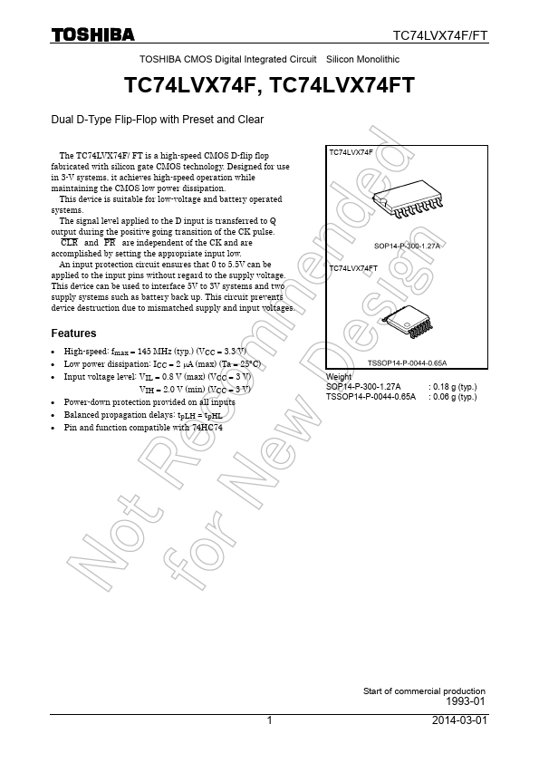
TC74LVX74F,TC74LVX74FN,TC74LVX74FT Dual D-Type Flip-Flop with Preset and Clear 
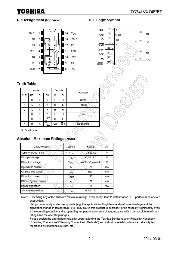
The TC74LVX74F/ FN/ FT is a high-speed CMOS D-flip flop fabricated with silicon gate CMOS technology. Designed for use in 3-V systems, it achieves high-speed operation while maintaining the CMOS low power dissipation. This device is suitable for low-voltage and battery operated systems. The signal level applied to the D input is transferred to Q output during the positive going transition of the CK pulse. CLR and PR are independent of the CK and are accomplished by setting the appropriate input low. An input protection circuit ensures that 0 to 5.
Published: |