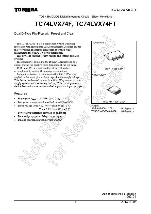
Datasheet4U Logo Datasheet4U.com

TC74LVX74FT - Dual D-Type Flip-Flop

This page provides the datasheet information for the TC74LVX74FT, a member of the TC74LVX74F Dual D-Type Flip-Flop family.

Features

  • High-speed: fmax = 145 MHz (typ. ) (VCC = 3.3 V).
  • Low power dissipation: ICC = 2 μA (max) (Ta = 25°C).
  • Input voltage level: VIL = 0.8 V (max) (VCC = 3 V) VIH = 2.0 V (min) (VCC = 3 V).
  • Power-down protection provided on all inputs.
  • Balanced propagation delays: tpLH ∼.
  • tpHL.
  • Pin and function compatible with 74HC74 TC74LVX74F TC74LVX74FT Weight SOP14-P-300-1.27A TSSOP14-P-0044-0.65A : 0.18 g (typ. ) : 0.06 g (typ. ) Start of commercia.

📥 Download Datasheet

Datasheet preview – TC74LVX74FT
Other Datasheets by Toshiba Semiconductor

Full PDF Text Transcription

Click to expand full text
TC74LVX74F/FT TOSHIBA CMOS Digital Integrated Circuit Silicon Monolithic TC74LVX74F, TC74LVX74FT Dual D-Type Flip-Flop with Preset and Clear The TC74LVX74F/ FT is a high-speed CMOS D-flip flop fabricated with silicon gate CMOS technology. Designed for use in 3-V systems, it achieves high-speed operation while maintaining the CMOS low power dissipation. This device is suitable for low-voltage and battery operated systems. 
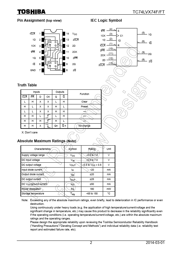
The signal level applied to the D input is transferred to Q output during the positive going transition of the CK pulse. CLR and PR are independent of the CK and are accomplished by setting the appropriate input low. An input protection circuit ensures that 0 to 5.5V can be applied to the input pins without regard to the supply voltage.
Published: |