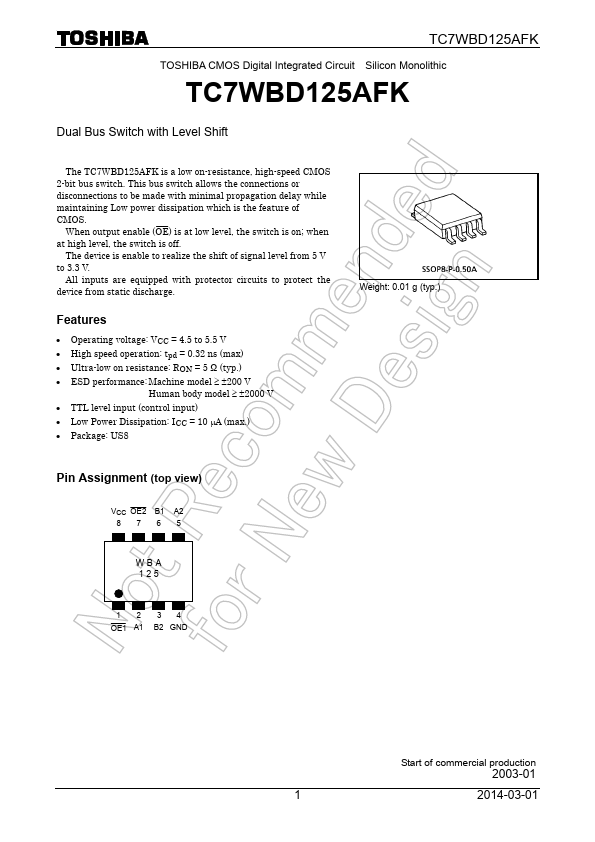
TC7WBD125AFK
feature of CMOS.
When output enable (OE) is at low level, the switch is on; when at high level, the switch is off.
The device is enable to realize the shift of signal level from 5 V to 3.3 V.
All inputs are equipped with protector circuits to protect the device from static discharge.
Features
- Operating voltage: VCC = 4.5 to 5.5 V
- High speed operation: tpd = 0.32 ns (max)
- Ultra-low on resistance: RON = 5 Ω (typ.)
- ESD performance: Machine model ≥ ±200 V
Human body model ≥ ±2000 V
- TTL level input (control input)
- Low Power Dissipation: ICC = 10 μA (max.)
- Package: US8
Weight: 0.01 g (typ.)
Pin Assignment (top view)
VCC OE2 B1 A2 8765
WBA 125
12 34 OE1 A1 B2 GND
Start of mercial production
2003-01
2014-03-01
Truth Table
Inputs OE L H
Function
A port = B port Disconnect
System Diagram
A1
B1
A2
B2
OE1
OE2
Absolute Maximum Ratings (Note)
Characteristics
Symbol
Rating
Unit
Power supply voltage Control pin input voltage Switch terminal I/O...