Description
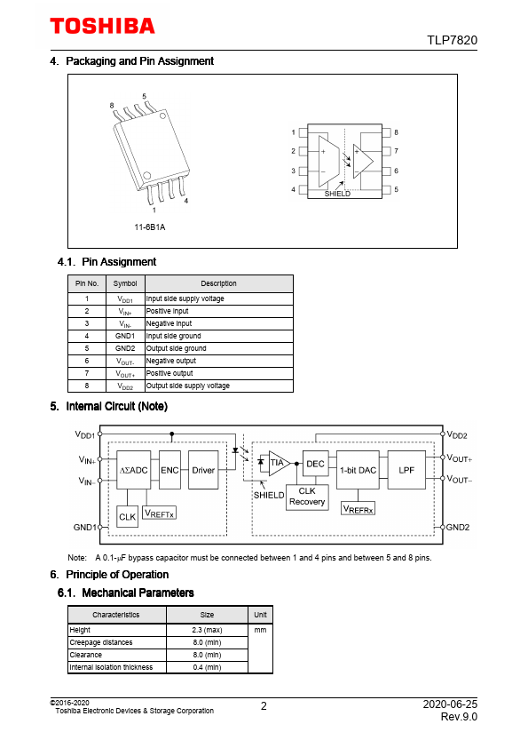
VDD1 VIN+ VINGND1 GND2 VOUTVOUT+ VDD2
Input side supply voltage Positive input Negative input Input side ground Output side ground Negative output Positive output Output side supply voltage
5. Internal Circuit (Note)
Note: A 0.1-µF bypass capacitor must be connected between 1 and 4 pins and between 5 and 8 pins.6. Principle of Operation 6.1. Mechanical Parameters
Characteristics
Height Creepage distances Clearance Internal isolation thickness
Size
Unit
2.3 (max)
mm
8.0 (min)
8.0 (min
Features
- (1) Gain accuracy: ±0.5 % (Gain rank B) (2) Gain drift: 0.00012 V/V/ (typ. ) (3) Nonlinearity (VIN = ±200 mV): 0.02 % (typ. ) (4) Input offset voltage: 0.9 mV (typ. ) (5) VOUT bandwidth (-3 dB): 230 kHz (typ. ) (6) Operating temperature range: -40 to 105 (7) Common-mode transient immunity: 15 kV/µs (min) (8) Safety standards
UL-recognized: UL 1577, File No. E67349 cUL-recognized: CSA Component Acceptance Service No.5A File No. E67349 VDE-approved: EN 60747-5-5, EN 62368-1 (Note 1) CQC-approved: GB4.