Datasheet Details
| Part number | TF3420 |
|---|---|
| Manufacturer | Tuofeng Semiconductor |
| File Size | 375.63 KB |
| Description | N-Channel Enhancement Mode Field Effect Transistor |
| Datasheet |
 TF3420 Datasheet TF3420 Datasheet
|
|
|
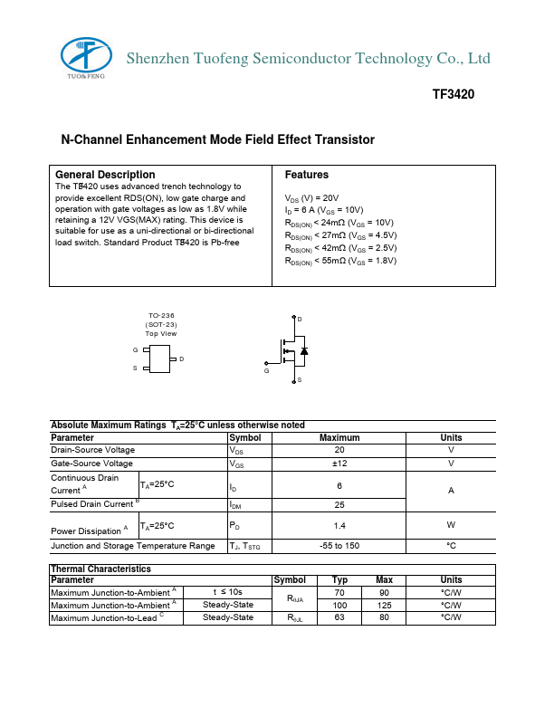
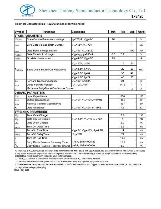
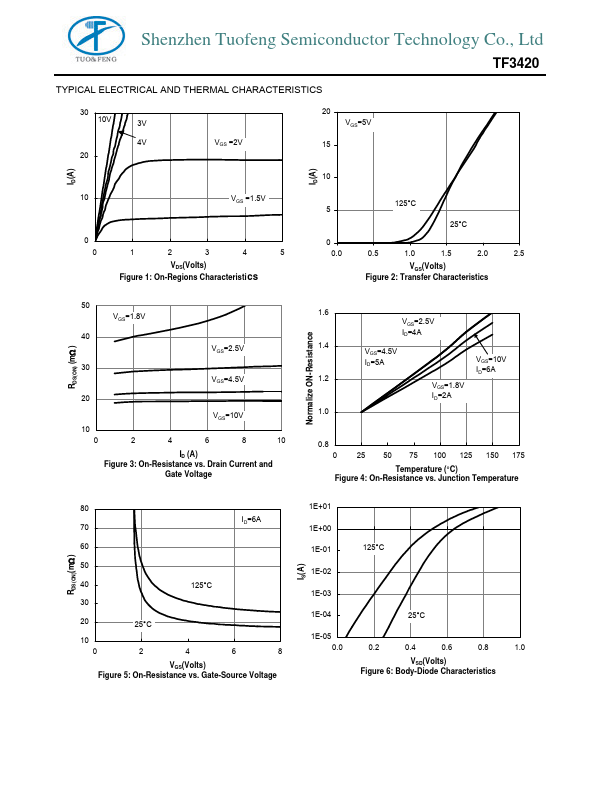
The TF3420 uses advanced trench technology to provide excellent RDS(ON), low gate charge and operation with gate voltages as low as 1.8V while retaining a 12V VGS(MAX) rating.
This device is suitable for use as a uni-directional or bi-directional load switch.
| Part number | TF3420 |
|---|---|
| Manufacturer | Tuofeng Semiconductor |
| File Size | 375.63 KB |
| Description | N-Channel Enhancement Mode Field Effect Transistor |
| Datasheet |
TF3420 Datasheet
|
|
|
|
| Part Number | Description | Manufacturer |
|---|---|---|
| TF341 | TO-220 3A Thyristor | Sanken electric |
| TF341M | TO-220 3A Thyristor | Sanken electric |
| TF341M-A | TO-220 3A High sensitive Thyristor | Sanken electric |
| TF341S | TO-220F 3A Thyristor | Sanken electric |
| TF3 | Solid Tantalum Surface Mount Chip Capacitors | Vishay |
| Part Number | Description |
|---|
The following content is an automatically extracted verbatim text from the original manufacturer datasheet and is provided for reference purposes only.