
Datasheet Details
| Part number | AO6802 |
|---|---|
| Manufacturer | UMW |
| File Size | 258.06 KB |
| Description | Dual 30V N-ChanneI MOSFET |
| Download | AO6802 Download (PDF) |
|
|
| Part number | AO6802 |
|---|---|
| Manufacturer | UMW |
| File Size | 258.06 KB |
| Description | Dual 30V N-ChanneI MOSFET |
| Download | AO6802 Download (PDF) |
|
|
|
The AO6802 uses advanced trench technology to provide excellent RDS(ON) and low gate charge.
This device is suitable for use as a load switch or in PWM applications.
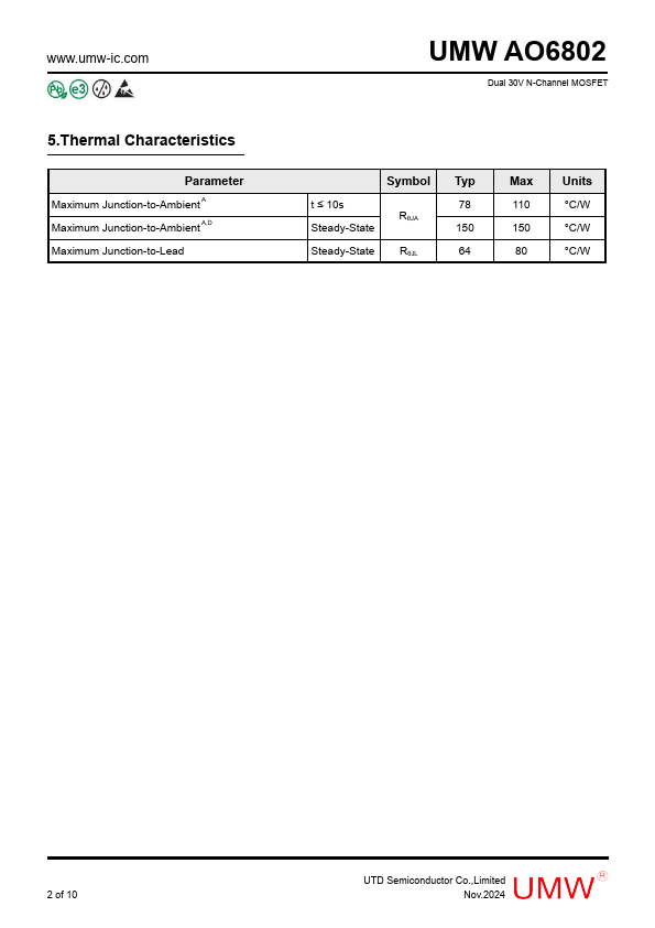
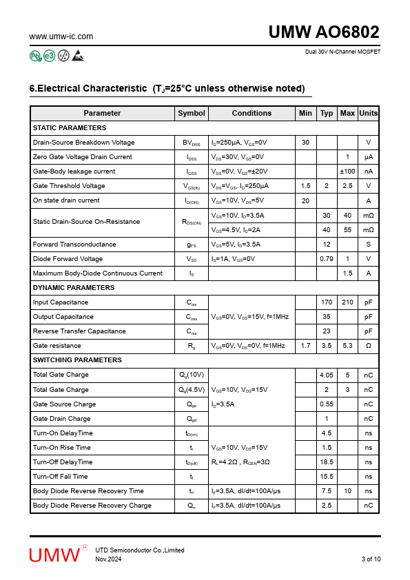
2.Product Summary VDS (V)=30V RDS(ON)<40mΩ(VGS=10V) RDS(ON)<55mΩ(VGS=4.5V) 3.Pinning information Pin Symbol Description 1,3 G1, G2 GATE 5,2 S1, S2 SOURCE 6,4 D1, D2 DRAIN D1 D2 G1 1 6 D1 S2 2 5 S1 G2 3 4 D2 G1 G2 S1 S2 SOT23-6 4.Absolute Maximum Ratings TA= 25°C Drain-Source Voltage Gate-Source Voltage Parameter Continuous Drain Current Pulsed Drain Current C Power Dissipation B Junction and Storage Temperature Range TA=25°C TA=70°C TA=25°C TA=70°C Symbol VDS VGS ID IDM PD TJ, TSTG Maximum 30 ±20 3.5 3 20 1.15 0.73 -55 to 150 Units V V A W W °C UTD Semiconductor Co.,Limited www.umw-ic.com Nov.2024 1 of 10 www.umw-ic.com 5.Thermal Characteristics Parameter Maximum Junction-to-Ambient A Maximum Junction-to-Ambient A,D Maximum Junction-to-Lead UMW AO6802 Dual 30V N-ChanneI MOSFET Symbol Typ t ≤ 10s 78 RθJA Steady-State 150 Steady-State RθJL 64 Max 110 150 80 Units °C/W °C/W °C/W 2 of 10 UTD Semiconductor Co.,Limited Nov.2024 www.umw-ic.com UMW AO6802 Dual 30V N-ChanneI MOSFET 6.Electrical Characteristic (TJ=25°C unless otherwise noted) Parameter STATIC PARAMETERS Drain-Source Breakdown Voltage Zero Gate Voltage Drain Current Gate-Body leakage current Gate Threshold Voltage On state drain current Static Drain-Source On-Resistance Forward Transconductance Diode Forward Voltage Maximum Body-Diode Continuous Current DYNAMIC PARAMETERS Input Capacitance Output Capacitance Reverse Transfer Capacitance Gate resistance SWITCHING PARAMETERS Total Gate Charge Total Gate Charge Gate Source Charge Gate Drain Charge Turn-On DelayTime Turn-On Rise Time Turn-Off DelayTime Turn-Off Fall Time Body Diode Reverse Recovery Time Body Diode Reverse Recovery Charge Symbol Conditions Min Typ Max Units BVDSS IDSS IGSS V
UMW AO6802 Dual 30V N-ChanneI MOSFET 1.
| Brand Logo | Part Number | Description | Manufacturer |
|---|---|---|---|
| AO6802 | Dual N-Channel MOSFET | Kexin | |
| AO6802 | N-Channel MOSFET | Freescale | |
| AO6802 | 30V Dual N-Channel MOSFET | Alpha & Omega Semiconductors |
| Part Number | Description |
|---|