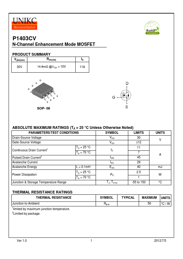
- Part: P1403CV
- Description: N-Channel MOSFET
- Manufacturer: UNIKC
- Size: 439.27 KB
Other P1403CV Datasheets
| Manufacturer | Part Number | Description |
|---|---|---|
| P1403EV8 | P-Channel FET | |
| P1403EV8 | P-Channel MOSFET | |
| P1403EVG | P-Channel FET |
| Manufacturer | Part Number | Description |
|---|---|---|
| P1403EV8 | P-Channel FET | |
| P1403EV8 | P-Channel MOSFET | |
| P1403EVG | P-Channel FET |