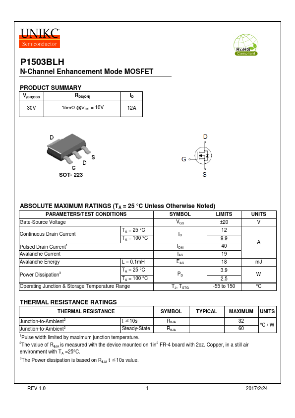
The following content is an automatically extracted verbatim text
from the original manufacturer datasheet and is provided for reference purposes only.
View original datasheet text
P1503BLH
N-Channel Enhancement Mode MOSFET
PRODUCT SUMMARY
V(BR)DSS
RDS(ON)
30V 15mΩ @VGS = 10V
ID 12A
SOT- 223
ABSOLUTE MAXIMUM RATINGS (TA = 25 °C Unless Otherwise Noted)
PARAMETERS/TEST CONDITIONS
SYMBOL
LIMITS
Gate-Source Voltage
VGS ±20
Continuous Drain Current Pulsed Drain Current1
TA = 25 °C TA = 100 °C
ID IDM
12 9.9 40
Avalanche Current
IAS 19
Avalanche Energy
L = 0.1mH
EAS
18
Power Dissipation3
TA = 25 °C TA = 100 °C
PD
3.9 2.5
Operating Junction & Storage Temperature Range
TJ, TSTG
-55 to 150
UNITS V
A
mJ W °C
THERMAL RESISTANCE RATINGS
THERMAL RESISTANCE
SYMBOL
TYPICAL MAXIMUM
Junction-to-Ambient2
t ≦10s
RqJA
32
Junction-to-Ambient2
Steady-State
RqJA
60
1Pulse width limited by maximum junction temperature.