P2610ATG Description
SYMBOL RθJC RθJA RθCS TYPICAL 0.5 MAXIMUM UNITS 0.97 62.5 °C / W Ver 1.0 1 2011/4/8 P2610ATG N-Channel Enhancement Mode MOSFET (TJ = 25 °C, Unless Otherwise Noted) PARAMETER SYMBO.
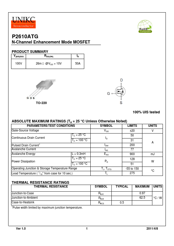
P2610ATG is N-Channel MOSFET manufactured by UNIKC.
| Manufacturer | Part Number | Description |
|---|---|---|
| P2610ADG | N-Channel Transistor | |
| P2610ASG | N-Channel MOSFET | |
| P2610BT | N-Channel Transistor | |
| P2610BTF | N-Channel Transistor |
SYMBOL RθJC RθJA RθCS TYPICAL 0.5 MAXIMUM UNITS 0.97 62.5 °C / W Ver 1.0 1 2011/4/8 P2610ATG N-Channel Enhancement Mode MOSFET (TJ = 25 °C, Unless Otherwise Noted) PARAMETER SYMBO.