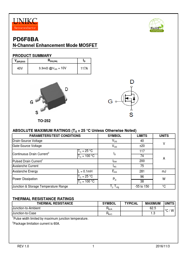
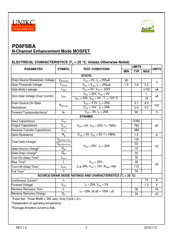
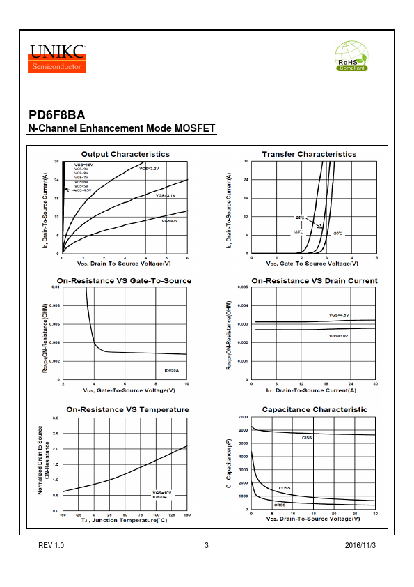
Click to expand full text
PD6F8BA
N-Channel Enhancement Mode MOSFET
PRODUCT SUMMARY
V(BR)DSS
RDS(ON)
40V 3.3mΩ @VGS = 10V
ID 117A
TO-252
ABSOLUTE MAXIMUM RATINGS (TA = 25 °C Unless Otherwise Noted)
PARAMETERS/TEST CONDITIONS
SYMBOL
LIMITS
Drain-Source Voltage
VDS 40
Gate-Source Voltage
VGS ±20
Continuous Drain Current2 Pulsed Drain Current1
TC = 25 °C TC = 100 °C
ID IDM
117 74 200
Avalanche Current
IAS 75
Avalanche Energy
L = 0.1mH
EAS
281
Power Dissipation
TC = 25 °C TC = 100 °C
PD
96 38
Junction & Storage Temperature Range
Tj, Tstg
-55 to 150
UNITS V
A
mJ W °C
THERMAL RESISTANCE RATINGS
THERMAL RESISTANCE Junction-to-Ambient
Junction-to-Case 1Pulse width limited by maximum junction temperature. 2Package limitation current is 60A.
SYMBOL RqJA RqJC
TYPICAL
MAXIMUM 62.5 1.