6N40-TC
Description
The N-Channel enhancement mode silicon gate power MOSFET is designed for high voltage, high speed power switching applications such as switching regulators, switching converters, solenoid, motor drivers, relay drivers.
Key Features
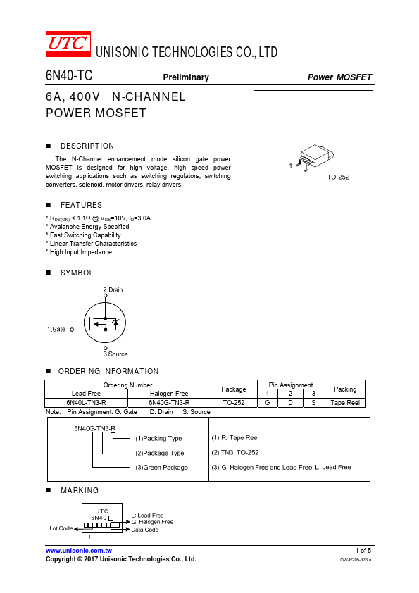
- SYMBOL Power MOSFET