75NM60
75NM60 is N-CHANNEL MOSFET manufactured by Unisonic Technologies.
DESCRIPTION
The UTC 75NM60 is a Super Junction MOSFET Structure and is designed to have better characteristics, such as fast switching time, low gate charge, low on-state resistance and a high rugged avalanche characteristics. This power MOSFET is usually used at DC-DC, AC-DC converters for power applications.
- FEATURES
- RDS(ON) < 55mΩ @ VGS = 10V, ID = 37.5A
- Fast switching capability
- Avalanche energy tested
- Improved dv/dt capability, high ruggedness
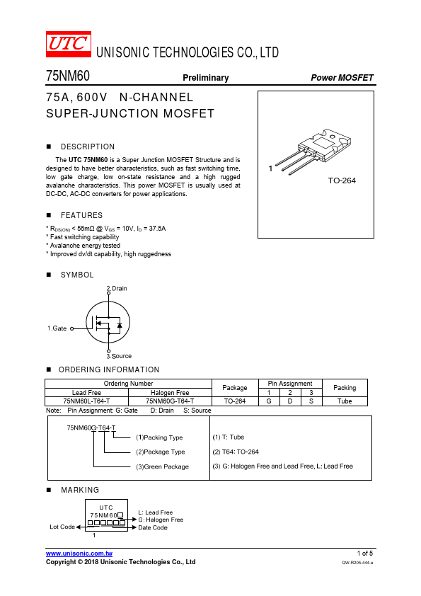
- SYMBOL
Power MOSFET
- ORDERING INFORMATION
Ordering Number
Lead Free
Halogen Free
75NM60L-T64-T
75NM60G-T64-T
Note: Pin Assignment: G: Gate D: Drain S: Source
Package TO-264
Pin Assignment 123 GDS
Packing Tube
- MARKING
.unisonic..tw Copyright © 2018 Unisonic Technologies Co., Ltd
1 of 5
QW-R205-444.a
Preliminary
Power MOSFET
- ABSOLUTE MAXIMUM RATINGS (TC =25°С, unless otherwise specified)
PARAMETER
SYMBOL
RATINGS
UNIT
Drain-Source Voltage
VDSS
Gate-Source Voltage
VGSS
±30
Drain Current
Continuous Pulsed (Note 2)
ID...