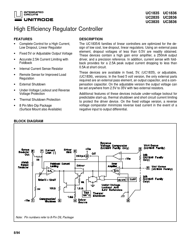
ABSOLUTE MAXIMUM RATINGS (Note 1)
Input Supply Voltage (+VIN) . . . . . . . . . . . . . . . . –1.0V to + 40V
Driver Output Current (Sink or Source) . . . . . . . . . . . . . 600mA
Driver Source to Sink Voltage . . . . . . . . . . . . . . . . . . . . . + 40V
Maximum Current Through Sense Resistor. . . . . . . . . . . . . . 4A
VOUT Sense Input Voltage . . . . . . . . . . . . . . . . . . –.3V to + 40V
Power Dissipation at TA = 25°C (Note 2) . . . . . . . . . . . 1000mW
Power Dissipation at TC = 25°C (Note 2) . . . . . . . . . . . 2000mW
CONNECTION DIAGRAMS
DIL-8, SOIC-8 (TOP VIEW)
N or J Package, D Package
SOIC-16 (TOP VIEW)
DW Package
UC1835 UC1836
UC2835 UC2836
UC3835 UC3836
Operating Junction Temperature . . . . . . . . . . . -55°C to +150°C
Storage Temperature . . . . . . . . . . . . . . . . . . . . -65°C to +150°C
Lead Temperature (Soldering, 10 Seconds) . . . . . . . . . . 300°C
Note 1: Voltages are referenced to ground, (Pin 3). Currents are
positive into, negative out of, the specified terminals.
Consult Packaging Section of Databook for thermal
considerations and limitations of packages.
PLCC-20, LCC-20
(TOP VIEW)
Q, L Packages
PACKAGE PIN FUNCTION
FUNCTION
PIN
N/C 1
+VIN
2
+VIN
3
N/C 4
Compensation/
Shutdown
5
N/C 6
Ground
7
N/C 8
N/C 9
Driver Source
10
N/C 11
VOUT Sense
12
N/C 13
N/C 14
Driver Sink
15
N/C 16
Current Limit (-)
17
N/C 18
Sense Resistor Out 19
Sense Resistor Out 20
ELECTRICAL CHARACTERISTICS: Unless otherwise stated, specifications hold for TA = 0°C to + 70°C for the
UC3835/6, –25°C to + 85°C for the UC2835/6, and –55°C to +125°C for the
UC1835/6, +VIN = 6V, Driver Source= 0V, Driver Sink = 5V, TA = TJ.
PARAMETER
TEST CONDITIONS
Input Supply
Supply Current
+VIN = 6V
+VIN = 40V
UVLO Threshold
+VIN Low to High, VOUT Sense = 0V
Threshold Hysteresis
Reverse Current
+VIN = -1.0V, Driver Sink Open
Regulating Voltage and Error Amplifier (UC1835 Family Only)
Regulating Level at VOUT Sense (VREG)
Driver Current = 10mA, TJ = 25°C
Over Temperature
Line Regulation
+VIN = 5.2V + 35V
Load Regulation
Driver Current = 0 to 250mA
Bias Current at VOUT Sense
VOUT Sense = 5.0V
Error Amp Transconductance
±100µA at Compensation/Shutdown Pin
Maximum Compensation Output Current
Sink or Source, Driver Source Open
MIN. TYP. MAX. UNITS
2.75 4.0 mA
3.75 6.0 mA
3.9 4.4 4.9 V
0.1 0.35 V
6.0 20 mA
4.94 5.0 5.06 V
4.9 5.1 V
15 40 mV
6.0 25 mV
75 125 210 µA
0.8 1.3 2.0 mS
90 200 260 µA
2