Si4826DY
Si4826DY is Dual N-Channel MOSFET manufactured by Vishay.
Vishay Siliconix
Asymmetrical Dual N-Channel 30-V (D-S) MOSFET
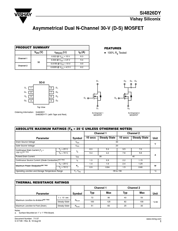
PRODUCT SUMMARY
Channel-1 Channel-2
VDS (V)
30 rDS(on) (W)
0.022 @ VGS = 10 V 0.030 @ VGS = 4.5 V 0.0155 @ VGS = 10 V 0.0205 @ VGS = 4.5 V
ID (A)
6.3 5.4 9.5 8.2
Features
D 100% Rg Tested
S1 1 G1 2 S2 3 G2 4
SO-8
8 D1 7 D2 6 D2 5 D2
Top View
Ordering Information: Si4826DY Si4826DY-T1 (with Tape and Reel)
D1 D2 D2 D2
G1 G2
S1
N-Channel 1 MOSFET
S2
N-Channel 2...