T330P
T330P is Silicon PIN Photodiode manufactured by Vishay.
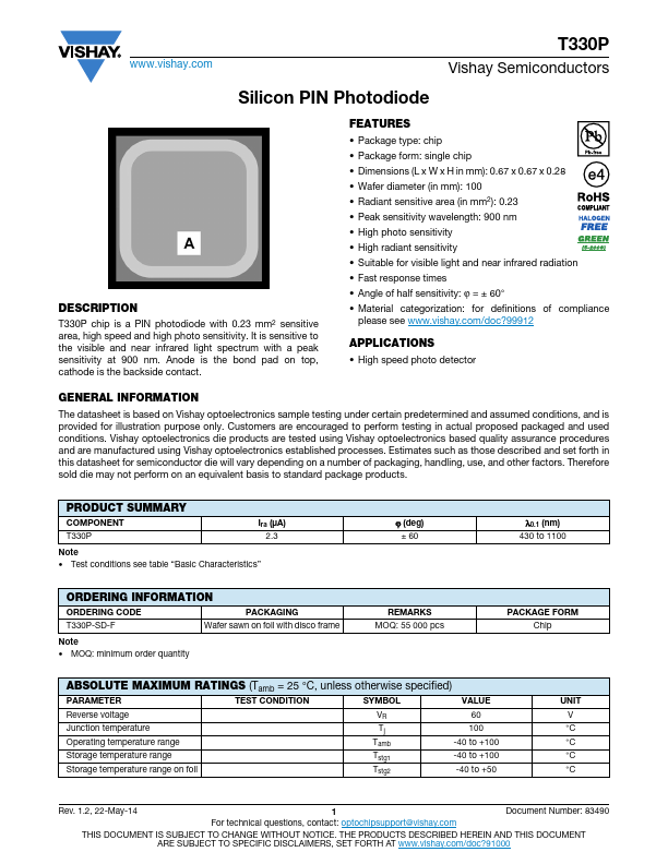
DESCRIPTION
T330P chip is a PIN photodiode with 0.23 mm2 sensitive area, high speed and high photo sensitivity. It is sensitive to the visible and near infrared light spectrum with a peak sensitivity at 900 nm. Anode is the bond pad on top, cathode is the backside contact.
FEATURES
- Package type: chip
- Package form: single chip
- Dimensions (L x W x H in mm): 0.67 x 0.67 x 0.28
- Wafer diameter (in mm): 100
- Radiant sensitive area (in mm2): 0.23
- Peak sensitivity wavelength: 900 nm
- High photo sensitivity
- High radiant sensitivity
- Suitable for visible light and near infrared radiation
- Fast response times
- Angle of half sensitivity: ϕ = ± 60°
- Material categorization: for definitions of pliance please see .vishay./doc?99912
APPLICATIONS
- High speed photo detector
GENERAL INFORMATION
The datasheet is based on Vishay optoelectronics sample testing under certain predetermined and assumed conditions, and is provided for illustration purpose only. Customers are encouraged to perform testing in actual proposed packaged and used conditions. Vishay optoelectronics die products are tested using Vishay optoelectronics based quality assurance procedures and are manufactured using Vishay optoelectronics established processes. Estimates such as those described and set forth in this datasheet for semiconductor die will vary depending on a number of packaging, handling, use, and other factors. Therefore sold die may not perform on an equivalent basis to standard package products.
PRODUCT SUMMARY
PONENT T330P
Ira (μA) 2.3
Note
- Test conditions see table “Basic Characteristics”
ϕ (deg) ± 60
λ0.1 (nm) 430 to 1100
ORDERING INFORMATION
ORDERING CODE
PACKAGING
T330P-SD-F
Wafer sawn on foil with disco frame
Note
- MOQ: minimum order quantity
REMARKS MOQ: 55 000 pcs
PACKAGE FORM Chip
ABSOLUTE MAXIMUM RATINGS (Tamb = 25 °C, unless otherwise specified)
PARAMETER
TEST CONDITION
SYMBOL
VALUE...