S505TXRW
Overview
- Easy Gate 1 switch-off with PNP switching transistors inside PLL e3
- High AGC-range with less steep slope
- Integrated gate protection diodes
- Low noise figure
- High gain, high forward transadmittance (30 mS typ.)
- Improved cross modulation at gain reduction
- SMD package
- Lead (Pb)-free component
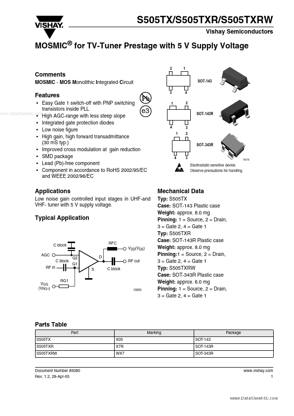
- Component in accordance to RoHS 2002/95/EC and WEEE 2002/96/EC 3 1 4 2 SOT-143R 4 1 3 2 SOT-343R 4 3 19216 Electrostatic sensitive device. Observe precautions for handling.