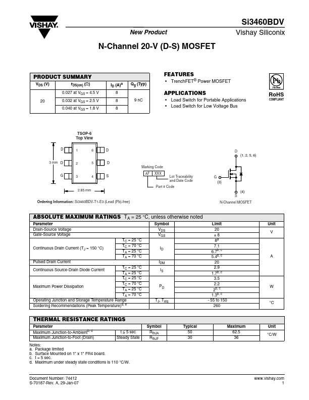
• Part: SI3460BDV
  • Description: N-Channel MOSFET
  • Category: MOSFET
  • Manufacturer: Vishay
  • Size: 176.36 KB
Download SI3460BDV Datasheet PDF
Vishay
SI3460BDV
SI3460BDV is N-Channel MOSFET manufactured by Vishay.
FEATURES - Trench FET® Power MOSFET APPLICATIONS - Load Switch for Portable Applications - Load Switch for Low Voltage Bus Ro HS PLIANT TSOP-6 Top View D 1 6 D D (1, 2, 5, 6) 3 mm D 2 5 D Marking Code G 3 4 S AF XXX Lot Traceability and Date Code Part # Code 2.85 mm S (4) N-Channel MOSFET G (3) Ordering Information: Si3460BDV-T1-E3 (Lead (Pb)-free) ABSOLUTE MAXIMUM RATINGS TA = 25 °C, unless otherwise noted Parameter Drain-Source Voltage Gate-Source Voltage Continuous Drain Current (TJ = 150 °C) Pulsed Drain Current Continuous Source-Drain Diode Current TC = 25 °C TA = 25 °C TC = 25 °C TC = 70 °C Maximum Power Dissipation TA = 25 °C TA = 70 °C Operating Junction and Storage Temperature Range Soldering Remendations (Peak Temperature)d, e TC = 25 °C TC = 70 °C TA = 25 °C TA = 70 °C Symbol VDS VGS ID IDM IS Limit 20 ±8 8a 7.1 6.7b, c 5.4b, c 20 2.9 1.7b, c 3.5 2.2 2b, c 1.3b, c - 55 to 150 260 Unit V PD TJ, Tstg °C THERMAL RESISTANCE RATINGS Parameter Maximum Junction-to-Ambientb, d Maximum Junction-to-Foot (Drain) t ≤ 5 sec Steady State Symbol Rth JA Rth JF Typical 50 30 Maximum 62.5 36 Unit °C/W Notes: a. Package limited b. Surface Mounted on 1" x 1" FR4 board. c. t = 5 sec. d. Maximum under steady state conditions is 110 °C/W. Document Number: 74412 S-70187-Rev. A, 29-Jan-07 .vishay. 1 Datasheet pdf - http://..net/ .Data Sheet.co.kr Vishay Siliconix SPECIFICATIONS TJ = 25 °C, unless otherwise noted Parameter Static Drain-Source Breakdown Voltage VDS Temperature Coefficient VGS(th) Temperature Coefficient Gate-Source Threshold Voltage Gate-Source Leakage Zero Gate Voltage Drain Current On-State Drain Currenta Drain-Source On-State Resistancea Forward Transconductancea Dynamic b Symbol VDS ΔVDS /TJ ΔVGS(th) /TJ VGS(th) IGSS IDSS ID(on) r DS(on) gfs Ciss Coss Crss Qg Qgs Qgd Rg td(on) tr td(off) tf td(on) tr td(off) tf IS ISM VSD trr Qrr ta tb Test Conditions VGS = 0 V, ID = 250 µA ID = 250 µA VDS = VGS , ID = 250 µA VDS = 0 V, VGS = ± 8 V VDS...