S904T
S904T is MOSMIC manufactured by Vishay.
S904T/S904TR
Vishay Telefunken
MOSMIC® for TV- Tuner Prestage with 9 V Supply Voltage
MOSMIC
- MOS Monolithic Integrated Circuit Electrostatic sensitive device. Observe precautions for handling.
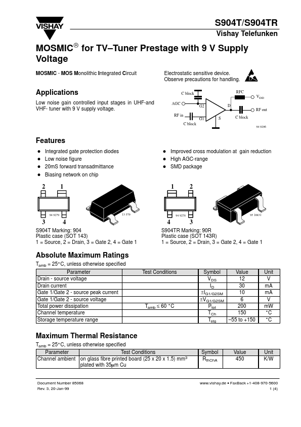
C block AGC RF in C block G2 G1 S D RF out C block
94 9296
Applications
Low noise gain controlled input stages in UHF-and VHF- tuner with 9 V supply voltage.
RFC VDD
Features
Integrated gate protection diodes Low noise figure 20mS forward transadmittance Biasing network on chip
D Improved cross modulation at gain reduction D High AGC-range D SMD package
1 2
94 9279
13 579
94 9278
95 10831
S904T Marking: 904 Plastic case (SOT 143) 1 = Source, 2 = Drain, 3 = Gate 2,...