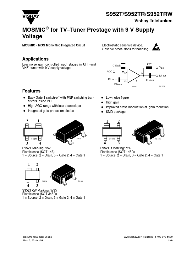
S952T/S952TR/S952TRW
Vishay Telefunken
Absolute Maximum Ratings
Tamb = 25_C, unless otherwise specified
Parameter
Drain - source voltage
Drain current
Gate 1/Gate 2 - source peak current
Gate 1/Gate 2 - source voltage
Total power dissipation
Channel temperature
Storage temperature range
Test Conditions
Tamb ≤ 60 °C
Symbol
VDS
ID
±IG1/G2SM
±VG1/G2SM
Ptot
TCh
Tstg
Value
12
30
10
6
200
150
–55 to +150
Unit
V
mA
mA
V
mW
°C
°C
Maximum Thermal Resistance
Tamb = 25_C, unless otherwise specified
Parameter
Test Conditions
Channel ambient on glass fibre printed board (25 x 20 x 1.5) mm3
mplated with 35 m Cu
Symbol
RthChA
Value
450
Unit
K/W
Electrical DC Characteristics
Tamb = 25_C, unless otherwise specified
Parameter
Test Conditions
Drain - source
m±IG1S = 10 A, VG2S = VG1S = 0
breakdown voltage
Gate 1 - source
±IG1S = 10 mA, VG2S = VDS = 0
breakdown voltage
Gate 2 - source
±IG2S = 10 mA, VG1S = VDS = 0
breakdown voltage
Gate 1 - source
leakage current
+VG1S = 5 V, VG2S = VDS = 0
Gate 2 - source
leakage current
Drain - source
operating current
Gate 1 - source
cut-off voltage
Gate 2 - source
cut-off voltage
±VG2S = 5 V, VG1S = VDS = 0
WVDS = VRG1 = 9 V, VG2S = 4 V, RG1 = 390 k
mVDS = VRG1 = 9 V, VG2S = 4 V, ID = 100 A
W mVDS = VRG1 = 9 V, RG1 = 390 k , ID = 100 A
Symbol Min Typ Max Unit
±V(BR)DSS 15
V
±V(BR)G1SS 7
10 V
±V(BR)G2SS 7
10 V
+IG1SS
20 nA
±IG2SS
20 nA
IDSO
7 10 14 mA
VG1S(OFF) 0.4
1.2 V
VG2S(OFF)
1.0
V
Remark on improving intermodulation behavior:
W WBy setting RG1 = 300 k instead of 390 k , typical value of IDSO will raise up to about 15 mA and improved inter-
modulation behavior will be performed.
www.vishay.de • FaxBack +1-408-970-5600
2 (6)
Document Number 85062
Rev. 3, 20-Jan-99