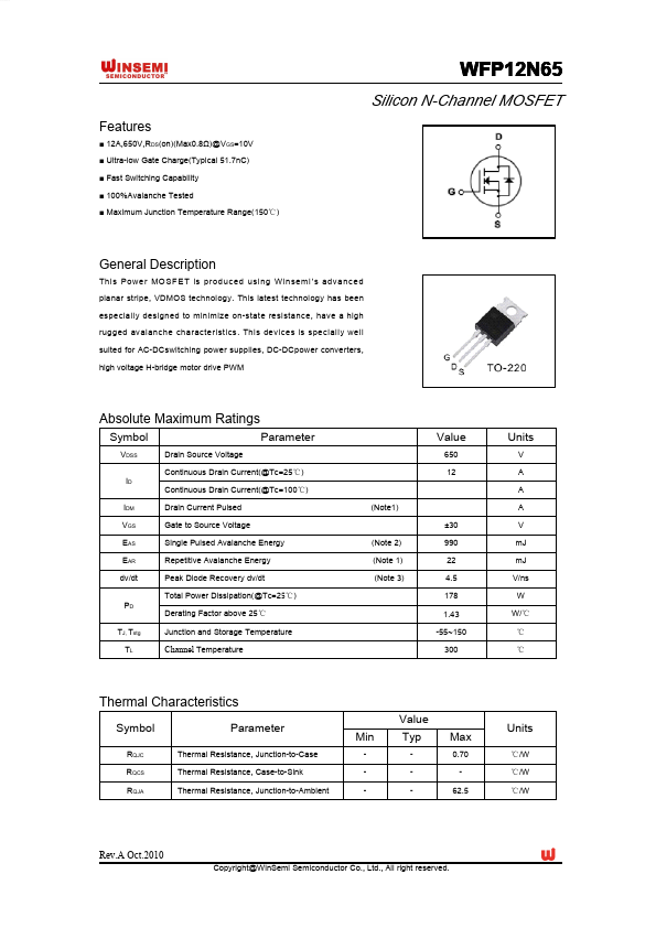
• Part: WFP12N65
  • Description: Silicon N-Channel MOSFET
  • Category: MOSFET
  • Manufacturer: WINSEMI SEMICONDUCTOR
  • Size: 635.33 KB
Download WFP12N65 Datasheet PDF
WINSEMI SEMICONDUCTOR
WFP12N65
WFP12N65 is Silicon N-Channel MOSFET manufactured by WINSEMI SEMICONDUCTOR.
Features - 12A,650V,RDS(on)(Max0.8Ω)@VGS=10V - Ultra-low Gate Charge(Typical 51.7n C) - Fast Switching Capability - 100%Avalanche Tested - Maximum Junction Temperature Range(150℃) General Description Thi s Pow e r MO SF ET is pr od u ced usi ng Wi n sem i ’s adv an ce d planar stripe, VDMOS technology. This latest technology has been especially designed to minimize on-state resistance, have a high rugged avalanche characteristics. This devices is specially well suited for AC-DCswitching power supplies, DC-DCpower converters, high voltage H-bridge motor drive PWM Absolute Maximum Ratings Symbol VDSS ID Continuous Drain Current(@Tc=100℃) IDM VGS EAS EAR dv/dt PD TJ, Tstg TL Drain Current Pulsed Gate to Source Voltage Single Pulsed Avalanche Energy Repetitive Avalanche Energy Peak Diode Recovery dv/dt Total Power Dissipation(@Tc=25℃) Derating Factor above 25℃ Junction and Storage Temperature (Note 2) (Note 1) (Note 3) (Note1) ±30 990 22 4.5 178 1.43 -55~150 300 A A V m J m J V/ns W W/℃ ℃ ℃ Drain Source Voltage Continuous Drain Current(@Tc=25℃) Parameter Value 650 12 Units Channel Temperature Thermal Characteristics Symbol RQJC RQCS RQJA Parameter Thermal Resistance, Junction-to-Case Thermal Resistance, Case-to-Sink Thermal Resistance, Junction-to-Ambient Value Min - Typ - Max 0.70 62.5 Units ℃/W ℃/W ℃/W Rev.A Oct.2010 Copyright@Win Semi Semiconductor Co., Ltd., All right reserved. .Data Sheet.in P12N6 5 WF WFP N65 Electrical Characteristics (Tc = 25°C) Characteristics Gate leakage current Gate- source breakdown voltage Drain cut- off current Drain- source breakdown voltage Gate threshold voltage Drain- source ON resistance Forward Transconductance Input capacitance Reverse transfer capacitance Output capacitance Rise time Turn- on time Switching time Fall time Turn- off time Total gate charge (gate- source Qg plus gate- drain) Gate- source charge Gate- drain (“miller”) Charge Qgs Qgd VGS = 10 V, n C ID = 12 A (Note4,5) 9.6 18.6 tf toff VDD = 520 V, 51.7 RG=25 Ω...