WJA1001
WJA1001 is 5V Active-Bias InGaP HBT Gain Block manufactured by WJ Communication.
Features
- 50
- 3000 MHz
- 19 d B Gain @ 900MHz
- +20 d Bm P1d B @ 900MHz ..
- +45 d Bm OIP3 @ 900MHz
- +5V Single Supply
- Low current draw (100 m A)
- Unconditionally stable
- Internally matched to 50
- Robust 1000V ESD, Class 1C
- Lead-free/green/Ro HS-pliant SOT-89 package
+5V Active-Bias In Ga P HBT Gain Block
Product Description
The WJA1001 is a cascadable gain block that offers high linearity in a low-cost surface-mount package. At 900 MHz, the WJA1001 typically provides 19 d B gain, +45 d Bm OIP3, and +20 d Bm P1d B. The device is housed in a leadfree/green/Ro HS-pliant SOT-89 SMT package using a Ni Pd Au plating to eliminate the possibility of tin whiskering. The WJA1001 consists of a Darlington-pair amplifier using a high reliability In Ga P/Ga As HBT process technology. The amplifier has been optimized internally to offer very high linearity performance at 1 GHz while drawing very low current. The MMIC amplifier is internally matched to 50Ω and only requires DC-blocking capacitors and a bias inductor for operation. An internal active bias is designed to enable stable performance over temperature and allow for operation directly from a +5V supply voltage. The broadband amplifier can be directly applied to various current and next generation wireless technologies such as GSM, CDMA, W-CDMA, Wi Bro, and Wi MAX. The WJA1001 is ideal for general purpose applications such as LO buffering or amplification and pre-driver stages within the 50 to 3000 MHz frequency range.
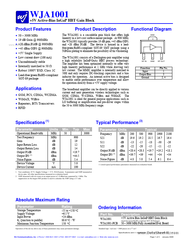
Functional Diagram
GND 4
1 RF IN
2 GND
3 RF OUT
Function Input Output/Bias Ground
Pin No. 1 3 2, 4
Applications
- -
- - GSM, PCS, CDMA, WCDMA Wi MAX, Wi Bro Repeaters, BTS Transceivers RFID
Specifications (1)
Parameter
Operational Bandwidth Test Frequency Gain Input Return Loss Output Return Loss Output P1d B Output IP3 (2) Noise Figure Device Voltage Device Current
Typical Performance (3)
Units
MHz MHz d B d B d B d Bm d Bm d B V m A
Min
Typ
900 19 12 14 +19.7 +44.5 5.4 5.0 100
Max
Parameter...