• Part: WJA1025
  • Description: 5V Active-Bias InGaP HBT Gain Block
  • Manufacturer: WJ Communication
  • Size: 217.14 KB
Download WJA1025 Datasheet PDF
WJ Communication
WJA1025
WJA1025 is 5V Active-Bias InGaP HBT Gain Block manufactured by WJ Communication.
Features - Cascadable gain block - 50 - 4000 MHz - 17 d B Gain @ 1.9GHz .. - +15.5 d Bm P1d B @ 1.9GHz - +32 d Bm OIP3 @ 1.9GHz - Operates from +5V @ 60m A - Robust 1000V ESD, Class 1C
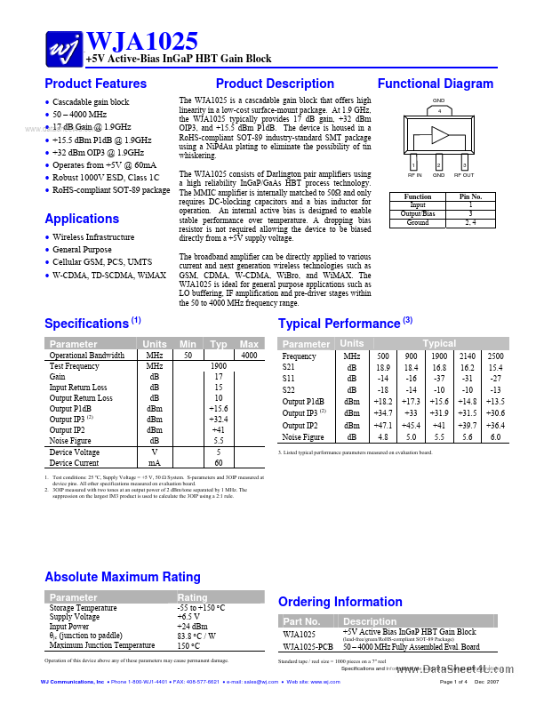
 - Ro HS-pliant SOT-89 package +5V Active-Bias In Ga P HBT Gain Block Product Description The WJA1025 is a cascadable gain block that offers high linearity in a low-cost surface-mount package. At 1.9 GHz, the WJA1025 typically provides 17 d B gain, +32 d Bm OIP3, and +15.5 d Bm P1d B. The device is housed in a Ro HS-pliant SOT-89 industry-standard SMT package using a Ni Pd Au plating to eliminate the possibility of tin whiskering. Functional Diagram GND 4 2 GND 3 RF OUT Applications - - - - Wireless Infrastructure General Purpose Cellular GSM, PCS, UMTS W-CDMA, TD-SCDMA, Wi MAX The WJA1025 consists of Darlington pair amplifiers using a high reliability In Ga P/Ga As HBT process technology. The MMIC amplifier is internally matched to 50Ω and only requires DC-blocking capacitors and a bias inductor for operation. An internal active bias is designed to enable stable performance over temperature. A dropping bias resistor is not required allowing the device to be biased directly from a +5V supply voltage. The broadband amplifier can be directly applied to various current and next generation wireless technologies such as GSM, CDMA, W-CDMA, Wi Bro, and Wi MAX. The WJA1025 is ideal for general purpose applications such as LO buffering, IF amplification and pre-driver stages within the 50 to 4000 MHz frequency range. RF IN Function Input Output/Bias Ground Pin No. 1 3 2, 4 Specifications (1) Parameter Operational Bandwidth Test Frequency Gain Input Return Loss Output Return Loss Output P1d B Output IP3 (2) Output IP2 Noise Figure Device Voltage Device Current Typical Performance (3) Units MHz MHz d B d B d B d Bm d Bm d Bm d B V m A Min Typ 1900 17 15 10 +15.6 +32.4 +41 5.5 5 60 Max Parameter Units Frequency S21 S11 S22 Output P1d B Output IP3 (2) Output IP2 Noise Figure MHz d B d B d B d Bm d Bm d Bm d...