Datasheet Summary
..
White Electronic Designs
ADVANCED-
2 Megabyte Sync/Sync Burst, Small Outline DIMM
Features
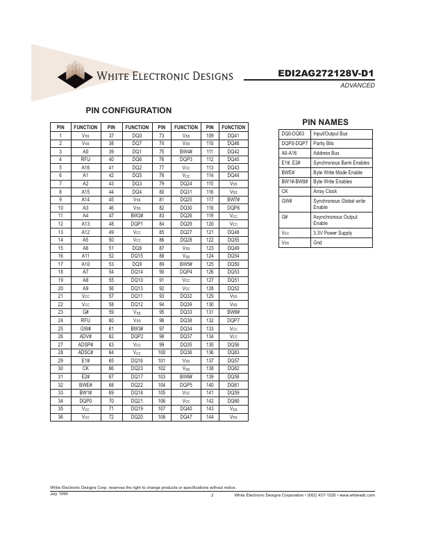
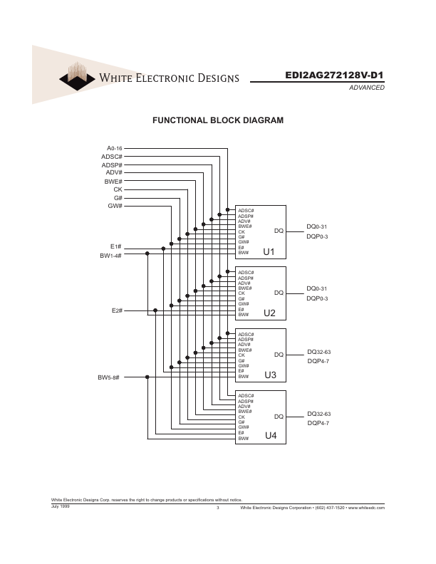
2x128Kx72 Synchronous, Synchronous Burst Flow-Through Architecture Linear Burst Mode Clock Controlled Registered Bank Enables (E1#, E2#) Clock Controlled Byte Write Mode Enable (BWE#) Clock Controlled Byte Write Enables (BW1#
- BW8#) Clock Controlled Registered Address Clock Controlled Registered Global Write (GW#) Aysnchronous Output Enable (G#) Internally self-timed Write Gold Lead Finish 3.3V ± 10% Operation Access Speed(s): TKHQV=8.5, 9, 10, 12ns mon Data I/O High Capacitance (30pf) drive, at rated Access Speed Single total array Clock Multiple Vcc and...