Datasheet4U Logo Datasheet4U.com

EDI2CG272128V - Sync/Sync Burst SRAM SO-DIMM

Description

The EDI2CG272128VxxD1 is a Synchronous/Synchronous Burst SRAM, 72 position DIMM (144 contacts) Module, small outline.

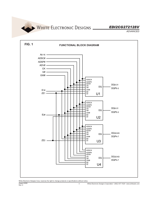
The Module contains four (4) Synchronous Burst Ram Devices, packaged in the industry standard JEDEC 14mmx20mm TQFP placed on a Multilayer FR4 Substrate.

Features

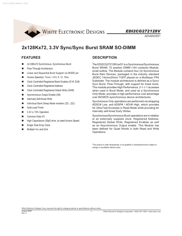
  • 2x128Kx72 Synchronous, Synchronous Burst Flow-Through Architecture Linear and Sequential Burst Support via MODE pin Access Speed(s): TKHQV = 8.5, 9, 12, 15ns Clock Controlled Registered Bank Enables (E1#, E2#) Clock Controlled Registered Address Clock Controlled Registered Global Write (GW#) Aysnchronous Output Enable (G#) Internally Self-timed Write Individual Bank Sleep Mode enables (ZZ1, ZZ2) Gold Lead Finish 3.3V ± 10% Operation Common Data I/O High Capacitance (30pf) drive, at rated Access.

📥 Download Datasheet

Datasheet Details

Part number EDI2CG272128V
Manufacturer White Electronic
File Size 190.78 KB
Description Sync/Sync Burst SRAM SO-DIMM
Datasheet download datasheet EDI2CG272128V Datasheet

Full PDF Text Transcription

Click to expand full text
www.DataSheet4U.com White Electronic Designs EDI2CG272128V ADVANCED* 2x128Kx72, 3.3V Sync/Sync Burst SRAM SO-DIMM FEATURES 2x128Kx72 Synchronous, Synchronous Burst Flow-Through Architecture Linear and Sequential Burst Support via MODE pin Access Speed(s): TKHQV = 8.5, 9, 12, 15ns Clock Controlled Registered Bank Enables (E1#, E2#) Clock Controlled Registered Address Clock Controlled Registered Global Write (GW#) Aysnchronous Output Enable (G#) Internally Self-timed Write Individual Bank Sleep Mode enables (ZZ1, ZZ2) Gold Lead Finish 3.
Published: |