WE128K32P-200G4MA
Representative WE128K32P-200G4MA image (package may vary by manufacturer)
Overview
- 66-pin, PGA Type, 27.3mm (1.075") square, Hermetic Ceramic HIP (Package 400)
- 68 lead, 40mm CQFP (G4), (Package 501)
- 68 lead, 22.4mm sq. CQFP (G2T), 4.57mm (0.180") high, (Package 509)
- 68 lead, 22.4mm sq. Low Profile CQFP (G1U), 3.57mm (0.140") high, (Package 519) s Organized as 128Kx32; User Configurable as 256Kx16 or 512Kx8 s Write Endurance 10,000 Cycles s Data Retention Ten Years Minimum (at +25°C) s Commercial, Industrial and Military Temperature Ranges s Low Power CMOS s Automatic Page Write Operation s Page Write Cycle Time: 10ms Max s Data Polling for End of Write Detection s Hardware and Software Data Protection s TTL Compatible Inputs and Outputs s 5 Volt Power Supply s Built-in Decoupling Caps and Multiple Ground Pins for Low Noise Operation s Weight WE128K32-XG2TX - 8 grams typical WE128K32-XG1UX - 5 grams typical WE128K32-XH1X - 13 grams typical WE128K32-XG4X - 20 grams typical
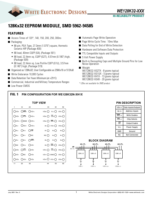
- 120ns not available for SMD product FIG. 1 PIN CONFIGURATION FOR WE128K32N-XH1X TOP VIEW 1 12 23 34 45 56 I/O8 WE2 I/O15 I/O24 VCC I/O31 I/O9 CS2 I/O14 I/O25 CS4 I/O30 I/O10 GND I/O13 I/O26 WE4 I/O29 A13 I/O11 I/O12 A6 I/O27 I/O28 A14 A10 OE A7 A3 A0 A15 A11 NC NC A4 A1 A16 A12 WE1 A8 A5 A2 NC VCC I/O7 A9 WE3 I/O23 I/O0 CS1 I/O6 I/O16 CS3 I/O22 I/O1 NC I/O5