Datasheet Summary
..
White Electronic Designs
EDI7F328XDNSN EDI7F2328XDNSN
ADVANCED-
8M x 32 / 2 x 8Mx 32; INTEL J3 BASED, FLASH
Features
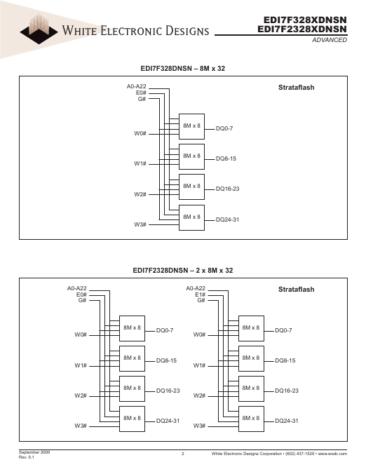
8M x 32 and 2 x 8M x 32 Densities Based on Intel’s Strataflash (J3) family of Flash Devices
- E28F640J3 (64) 128Kb Erase Blocks (Symetrical) High Performance Interface Async Page Mode Reads
- 120/25 ns Read Access Time 2.7V
- 3.6V Vcc Operation 128 bit Protection Register;
- 64 bit Unique Device Identifier
- 64 bit User Programmable OTP Cells mon Flash Interface (CFI) Scaleable mand Set (SCS) 32 byte Write Buffer, 64M Total Erase Cycles
- 100,000 Erase Cycles per Block Package
- 80 pin SIMM
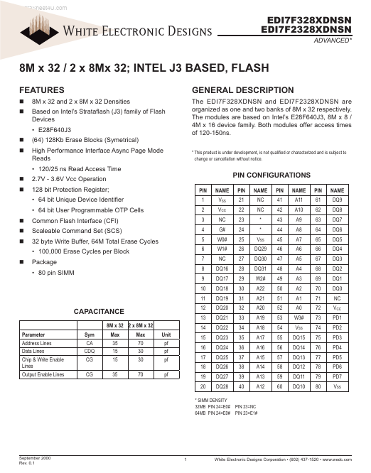
PIN 1 2 3 4 5 6 7 8 9 10 11 NAME VSS VCC NC G# W0# W1# NC...