• Part: WED3DL3216V
  • Description: 16Mx32 SDRAM
  • Manufacturer: White Electronic Designs
  • Size: 857.39 KB
Download WED3DL3216V Datasheet PDF
White Electronic Designs
WED3DL3216V
WED3DL3216V is 16Mx32 SDRAM manufactured by White Electronic Designs.
FEATURES 40% Space Savings vs. Monolithic Solution Reduced System Inductance and Capacitance 3.3V Operating Supply Voltage Fully Synchronous to Positive Clock Edge Clock Frequencies of 100MHz - 133MHz Burst Operation - Sequential or Interleave - Burst Length = Programmable 1, 2, 4, 8 or Full Page - Burst Read and Write - Multiple Burst Read and Single Write Data Mask Control Per Byte Auto and Self Refresh Automatic and Controlled Precharge mands Suspend Mode and Power Down Mode 119 Pin BGA, 17mm x 23mm DESCRIPTION 
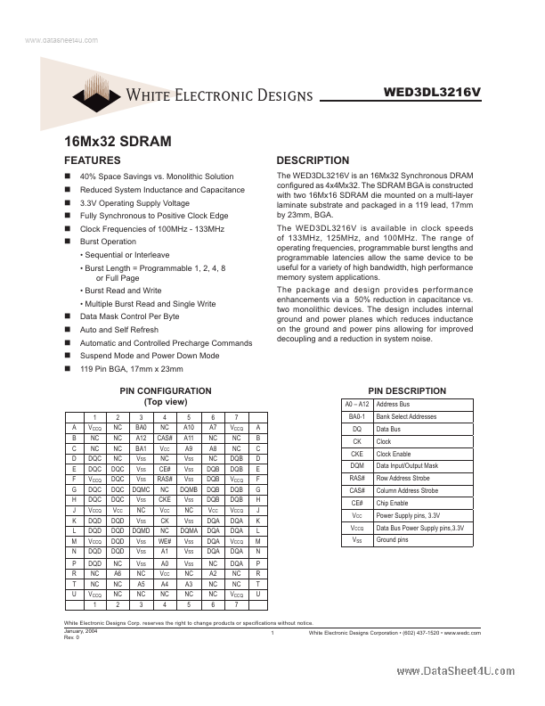
The WED3DL3216V is an 16Mx32 Synchronous DRAM configured as 4x4Mx32. The SDRAM BGA is constructed with two 16Mx16 SDRAM die mounted on a multi-layer laminate substrate and packaged in a 119 lead, 17mm by 23mm, BGA. The WED3DL3216V is available in clock speeds of 133MHz, 125MHz, and 100MHz. The range of operating frequencies, programmable burst lengths and programmable latencies allow the same device to be useful for a variety of high bandwidth, high performance memory system applications. The package and design provides performance enhancements via a 50% reduction in capacitance vs. two monolithic devices. The design includes internal ground and power planes which reduces inductance on the ground and power pins allowing for improved decoupling and a reduction in system noise. PIN CONFIGURATION (Top view) 1 A B C D E F G H J K L M N P R T U VCCQ NC NC DQC DQC VCCQ DQC DQC VCCQ DQD DQD VCCQ DQD DQD NC NC VCCQ 1 2 NC NC NC NC DQC DQC DQC DQC VCC DQD DQD DQD DQD NC A6 NC NC 2 3 4 BA0 NC A12 CAS# BA1 VCC NC VSS VSS CE# VSS RAS# DQMC NC CKE VSS NC VCC VSS CK DQMD NC VSS WE# VSS A1 VSS NC A5 NC 3 A0 VCC A4 NC 4 5 A10 A11 A9 VSS VSS VSS DQMB VSS NC VSS DQMA VSS VSS VSS NC A3 NC 5 6 A7 NC A8 NC DQB DQB DQB DQB VCC DQA DQA DQA DQA NC A2 NC NC 6 7 VCCQ NC NC DQB DQB VCCQ DQB DQB VCCQ DQA DQA VCCQ DQA DQA NC NC VCCQ 7 A B C D E F G H J K L M N P R T U PIN DESCRIPTION A0 - A12 BA0-1 DQ CK CKE DQM RAS# CAS# CE# VCC VCCQ VSS Address Bus Bank Select...