WSE128K16-xxx Overview
Key Features
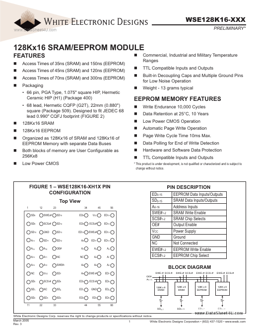
- 66 pin, PGA Type, 1.075" square HIP, Hermetic Ceramic HIP (H1) (Package
- 68 lead, Hermetic CQFP (G2T), 22mm (0.880") square (Package 509). Designed to fit JEDEC 68 lead 0.990" CQFJ footprint (FIGURE
| Part | WSE128K16-xxx |
|---|---|
| Description | 128Kx16 SRAM/EEPROM MODULE |
| Category | EEPROM |
| Manufacturer | White Electronic Designs Corporation |
| Size | 611.35 KB |
| Part Number | Manufacturer | Description |
|---|---|---|
| HFDOM40B-xxxSx | Hanbit Electronics | 40Pin Flash Disk Module |
| HFDOM44P-xxxSx | Hanbit Electronics | 44Pin Flash Disk Module |
| HFDOM40P-xxxSx | Hanbit Electronics | 40Pin Flash Disk Module |