WFF10N60
Features
- Low Intrinsic Capacitances
- Excellent Switching Characteristics
- Extended Safe Operating Area
- Unrivalled Gate Charge :Qg= 33n C (Typ.)
- BVDSS=600V,ID=10A
- RDS(on) :0.73 Ω (Max) @VG=10V
- 100% Avalanche Tested
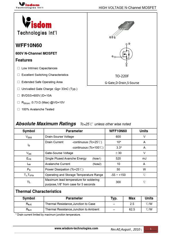
GD S
TO‐220F
G‐Gate,D‐Drain,S‐Sourse
Absolute Maximum Ratings Tc=25℃ unless other wise noted
Symbol
VDSS
VGS EAS IAR PD TJ,TSTG
Parameter
Drain-Sourse Voltage
Drain Current
-continuous (Tc=25℃)
-continuous (Tc=100℃)
Gate-Sourse Voltage
Single Plused Avanche Energy (Note1)
Avalanche Current
(Note2)
Power Dissipation (Tc=25℃)
Operating and Storage Temperature Range
Maximum lead temperature for soldering purpose,1/8” from case for 5 seconds
600 10- 3.3- ±30 520 10 50 -55 ~ +150
Units
V A A V m J A W...