Datasheet4U Logo Datasheet4U.com

XD272 - dual operational amplifiers

Datasheet Summary

Description

input offset voltage grades with low offset voltage drift, high input impedance, low noise, and speeds approaching that of general-purpose BiFET devices.

📥 Download Datasheet

Datasheet preview – XD272

Datasheet Details

Part number XD272
Manufacturer XINLUDA
File Size 375.26 KB
Description dual operational amplifiers
Datasheet download datasheet XD272 Datasheet
Additional preview pages of the XD272 datasheet.
Other Datasheets by XINLUDA

Full PDF Text Transcription

Click to expand full text
D Input Offset Voltage Drift . . . Typically 0.1 µV/Month, Including the First 30 Days D Wide Range of Supply Voltages Over Specified Temperature Range: 0°C to 70°C . . . 3 V to 16 V – 40°C to 85°C . . . 4 V to 16 V – 55°C to 125°C . . . 4 V to 16 V D Single-Supply Operation D Common-Mode Input Voltage Range Extends Below the Negative Rail (C-Suffix, I-Suffix types) D Low Noise . . . Typically 25 nV/√Hz at f = 1 kHz D Output Voltage Range Includes Negative Rail D High Input impedance . . . 1012 Ω Typ D ESD-Protection Circuitry description 
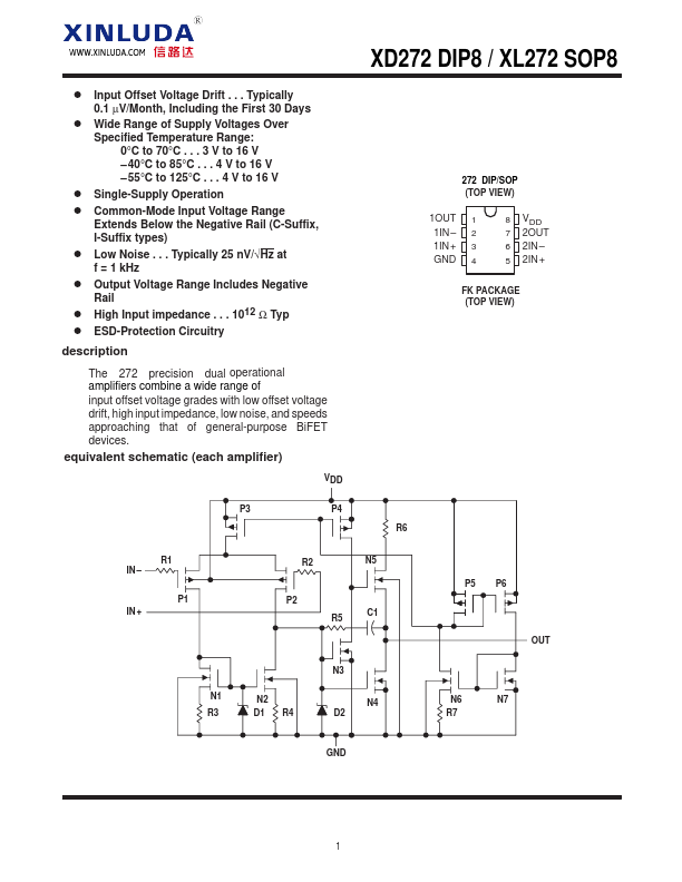
The 272 precision dual operational amplifiers combine a wide range of input offset voltage grades with low offset voltage drift, high input impedance, low noise, and speeds approaching that of general-purpose BiFET devices.
Published: |