Datasheet4U Logo Datasheet4U.com

XQ7VX485T - Virtex-7 T and XT FPGAs

Download the XQ7VX485T datasheet PDF. This datasheet also covers the XQ7V585T variant, as both devices belong to the same virtex-7 t and xt fpgas family and are provided as variant models within a single manufacturer datasheet.

General Description

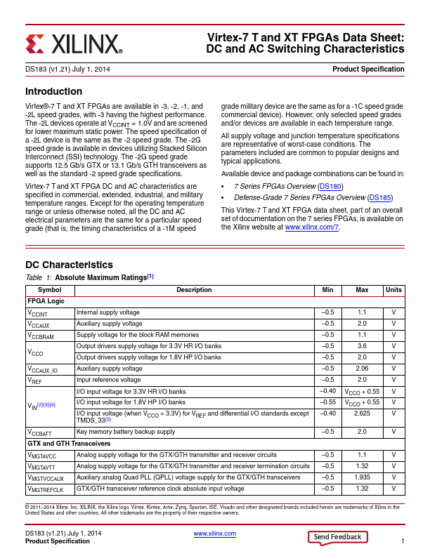
FPGA Logic VCCINT VCCAUX VCCBRAM VCCO Internal supply voltage Auxiliary supply voltage Supply voltage for the block RAM memories Output drivers supply voltage for 3.3V HR I/O banks Output drivers supply voltage for 1.8V HP I/O banks VCCAUX_IO VREF Auxiliary supply voltage Input reference voltag

Key Features

  • eristics Table 3: DC Characteristics Over Recommended Operating Conditions (Cont’d) Symbol.

📥 Download Datasheet

Note: The manufacturer provides a single datasheet file (XQ7V585T-Xilinx.pdf) that lists specifications for multiple related part numbers.

Full PDF Text Transcription (Reference)

The following content is an automatically extracted verbatim text from the original manufacturer datasheet and is provided for reference purposes only.

View original datasheet text
DS183 (v1.21) July 1, 2014 Virtex-7 T and XT FPGAs Data Sheet: DC and AC Switching Characteristics Product Specification Introduction Virtex®-7 T and XT FPGAs are available in -3, -2, -1, and -2L speed grades, with -3 having the highest performance. The -2L devices operate at VCCINT = 1.0V and are screened for lower maximum static power. The speed specification of a -2L device is the same as the -2 speed grade. The -2G speed grade is available in devices utilizing Stacked Silicon Interconnect (SSI) technology. The -2G speed grade supports 12.5 Gb/s GTX or 13.1 Gb/s GTH transceivers as well as the standard -2 speed grade specifications. Virtex-7 T and XT FPGA DC and AC characteristics are specified in commercial, extended, industrial, and military temperature ranges.