YJH03N10A Description
Pulse Width≤300us,Duty cycle ≤2%. Device mounted on FR-4 PCB, 1 inch x 0.85 inch x 0.062 inch. YJH03N10A Typical Performance Characteristics Figure1.
YJH03N10A is N-Channel Enhancement Mode Field Effect Transistor manufactured by Yangjie Electronic.
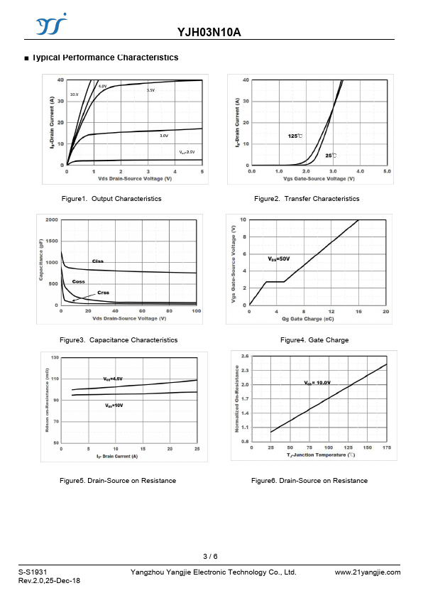
Pulse Width≤300us,Duty cycle ≤2%. Device mounted on FR-4 PCB, 1 inch x 0.85 inch x 0.062 inch. YJH03N10A Typical Performance Characteristics Figure1.