PDSP1601A Overview
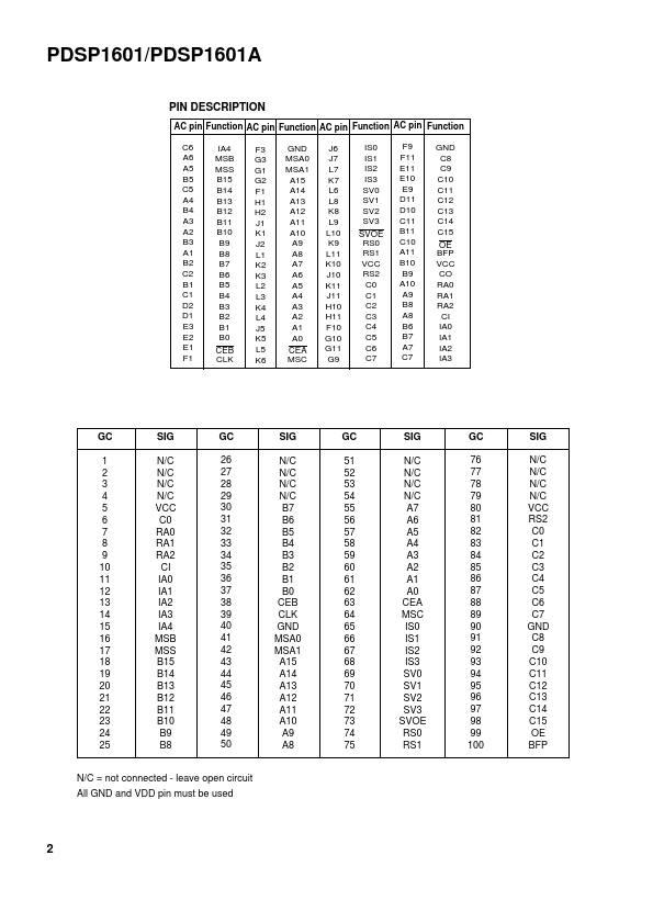
AC pin Function AC pin Function AC pin Function AC pin Function C6 A6 A5 B5 C5 A4 B4 A3 A2 B3 A1 B2 C2 B1 C1 D2 D1 E3 E2 E1 F1 IA4 MSB MSS B15 B14 B13 B12 B11 B10 B9 B8 B7 B6 B5 B4 B3 B2 B1 B0 CEB CLK F3 G3 G1 G2 F1 H1 H2 J1 K1 J2 L1 K2 K3 L2 L3 K4 L4 J5 K5.
PDSP1601A Key Features
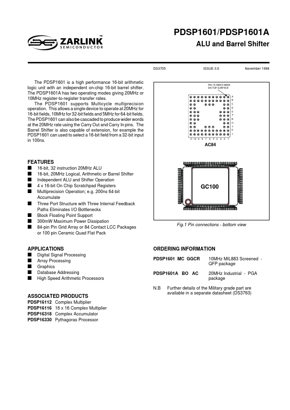
- bottom view