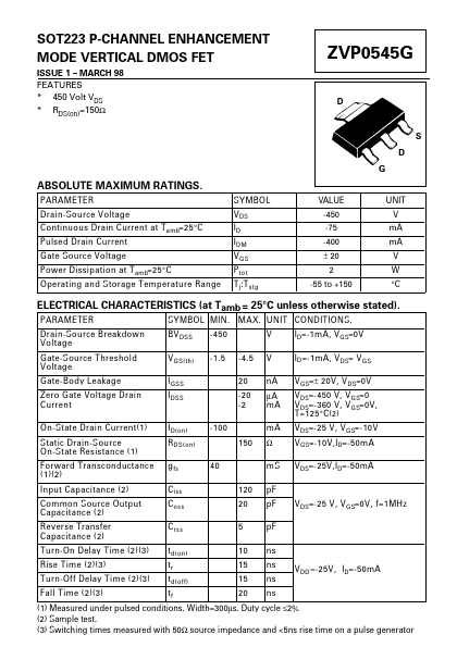
ZVP0545G
ZVP0545G is P-CHANNEL ENHANCEMENT MODE VERTICAL DMOS FET manufactured by Zetex Semiconductors.
FEATURES
- 450 Volt VDS
- RDS(on)=150Ω
ABSOLUTE MAXIMUM RATINGS.
PARAMETER Drain-Source Voltage Continuous Drain Current at T amb=25°C Pulsed Drain Current Gate Source Voltage Power Dissipation at T amb=25°C Operating and Storage Temperature Range SYMBOL V DS ID I DM V GS P tot T j :T stg VALUE -450 -75 -400 ± 20 2 -55 to +150 UNIT V m A m A V W °C
ELECTRICAL CHARACTERISTICS (at Tamb = 25°C unless otherwise stated).
PARAMETER Drain-Source Breakdown Voltage Gate-Source Threshold Voltage Gate-Body Leakage Zero Gate Voltage Drain Current On-State Drain Current(1) Static Drain-Source On-State Resistance (1) Forward Transconductance (1)(2) Input Capacitance (2) mon Source Output Capacitance (2) Reverse Transfer Capacitance (2) Turn-On Delay Time (2)(3) Rise Time (2)(3) Turn-Off Delay Time (2)(3) Fall Time (2)(3) SYMBOL MIN. BV DSS V GS(th) I GSS I DSS -450 -1.5 -4.5 20 -20 -2 -100 150 40 120 20 5 10 15 15 20 MAX. UNIT CONDITIONS. V V n A µA m A m A Ω m S p F p F p F ns ns ns ns V DD ≈ -25V, I D=-50m A V DS=-25 V, V GS=0V, f=1MHz I D=-1m A, V GS=0V I D =-1m A, V DS= V GS V GS= ± 20V, V DS=0V V DS=-450 V, V GS=0 V DS=-360 V, V GS=0V, T=125°C (2) V DS=-25 V, V GS=-10V V GS=-10V,I D=-50m A V DS=-25V,I D=-50m A
I D(on) R DS(on) g fs C iss C oss C rss t d(on) tr t d(off) tf
(1) Measured under pulsed conditions. Width=300µs. Duty cycle ≤2% (2) Sample test. (3) Switching times measured with 50Ω source impedance and <5ns rise time on a pulse...