74HC4066N Overview
Key Specifications
Package: PDIP
Mount Type: Through Hole
Pins: 14
Operating Voltage: 5 V
Description
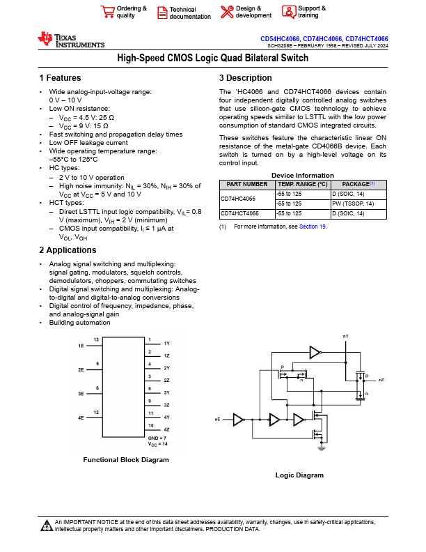
The ’HC4066 and CD74HCT4066 devices contain four independent digitally controlled analog switches that use silicon-gate CMOS technology to achieve operating speeds similar to LSTTL with the low power consumption of standard CMOS integrated circuits. These switches feature the characteristic linear ON resistance of the metal-gate CD4066B device.
Key Features
- Wide analog-input-voltage range: 0 V – 10 V
- Low ON resistance: – VCC = 4.5 V: 25 Ω – VCC = 9 V: 15 Ω
- Fast switching and propagation delay times
- Low OFF leakage current
- Wide operating temperature range: –55°C to 125°C