ADS4229
ADS4229 is Ultralow-Power ADC manufactured by Texas Instruments.
Features
- 1 Maximum Sample Rate: 250 MSPS
- Ultralow Power with Single 1.8-V Supply:
- 545-m W Total Power at 250 MSPS
- High Dynamic Performance:
- 80.8-d Bc SFDR at 170 MHz
- 69.4-d BFS SNR at 170 MHz
- Crosstalk: > 90 d B at 185 MHz
- Programmable Gain Up to 6 d B for SNR and SFDR Trade-off
- DC Offset Correction
- Output Interface Options:
- 1.8-V Parallel CMOS Interface
- DDR LVDS With Programmable Swing:
- Standard Swing: 350 m V
- Low Swing: 200 m V
- Supports Low Input Clock Amplitude Down to 200 m VPP
- Package: 9-mm × 9-mm, 64-Pin Quad Flat No-Lead (QFN) Package
3 Description
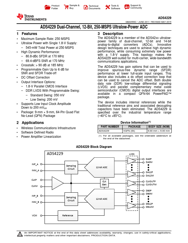
The ADS4229 is a member of the ADS42xx ultralowpower family of dual-channel, 12-bit and 14-bit analog-to-digital converters (ADCs). Innovative design techniques are used to achieve high dynamic performance, while consuming extremely low power with a 1.8-V supply. This topology makes the ADS4229 well-suited for multi-carrier, wide-bandwidth munications applications.
The ADS4229 has gain options that can be used to improve spurious-free dynamic range (SFDR) performance at lower full-scale input ranges. This device also includes a dc offset correction loop that can be used to cancel the ADC offset. Both double data rate (DDR) low-voltage differential signaling (LVDS) and parallel plementary metal oxide semiconductor (CMOS) digital output interfaces are available in a pact QFN-64 Power PAD™ package.
The device includes internal references while the traditional reference pins and associated decoupling capacitors have been eliminated. The ADS4229 is specified over the industrial temperature range (- 40°C to +85°C).
2 Applications
- Wireless munications Infrastructure
- Software Defined Radio
- Power Amplifier Linearization
Device Information(1)
PART NUMBER
PACKAGE
BODY SIZE (NOM)
VQFN (64)
9.00 mm × 9.00 mm
(1) For all available packages, see the orderable addendum at the end of the datasheet.
ADS4229 Block Diagram
INP_A INM_A
CLKP CLKM
INP_B INM_B
Sampling...