Datasheet4U Logo Datasheet4U.com

ADS42LB49 - Analog-to-Digital Converter

General Description

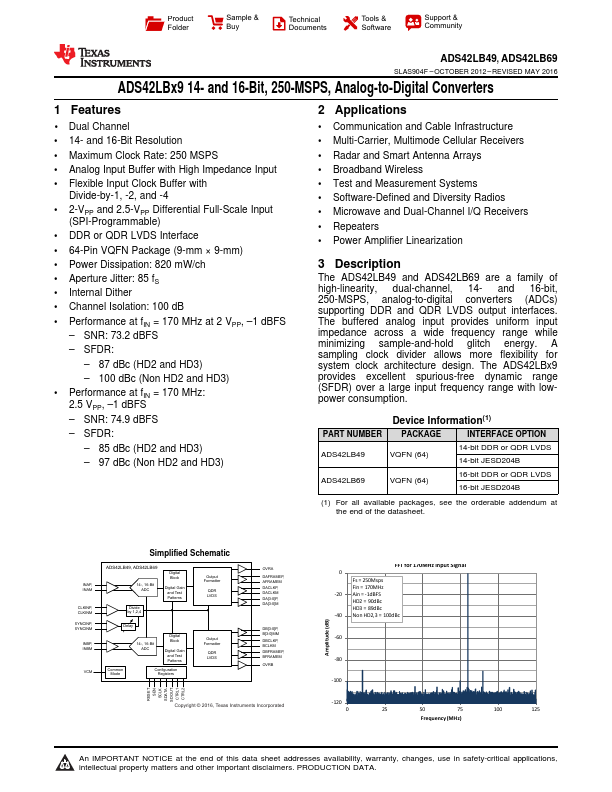
The ADS42LB49 and ADS42LB69 are a family of high-linearity, dual-channel, 14- and 16-bit, 250-MSPS, analog-to-digital converters (ADCs) supporting DDR and QDR LVDS output interfaces.

Key Features

  • 1 Dual Channel.
  • 14- and 16-Bit Resolution.
  • Maximum Clock Rate: 250 MSPS.
  • Analog Input Buffer with High Impedance Input.
  • Flexible Input Clock Buffer with Divide-by-1, -2, and -4.
  • 2-VPP and 2.5-VPP Differential Full-Scale Input (SPI-Programmable).
  • DDR or QDR LVDS Interface.
  • 64-Pin VQFN Package (9-mm × 9-mm).
  • Power Dissipation: 820 mW/ch.
  • Aperture Jitter: 85 fS.
  • Internal Dither.
  • Channel Isola.

📥 Download Datasheet

Full PDF Text Transcription (Reference)

The following content is an automatically extracted verbatim text from the original manufacturer datasheet and is provided for reference purposes only.

View original datasheet text
Product Folder Sample & Buy Technical Documents Tools & Software Support & Community ADS42LB49, ADS42LB69 SLAS904F – OCTOBER 2012 – REVISED MAY 2016 ADS42LBx9 14- and 16-Bit, 250-MSPS, Analog-to-Digital Converters 1 Features •1 Dual Channel • 14- and 16-Bit Resolution • Maximum Clock Rate: 250 MSPS • Analog Input Buffer with High Impedance Input • Flexible Input Clock Buffer with Divide-by-1, -2, and -4 • 2-VPP and 2.5-VPP Differential Full-Scale Input (SPI-Programmable) • DDR or QDR LVDS Interface • 64-Pin VQFN Package (9-mm × 9-mm) • Power Dissipation: 820 mW/ch • Aperture Jitter: 85 fS • Internal Dither • Channel Isolation: 100 dB • Performance at fIN = 170 MHz at 2 VPP, –1 dBFS – SNR: 73.