CD4066BQ
CD4066BQ is CMOS Quad Bilateral Switch manufactured by Texas Instruments.
- Part of the CD4066B-Q1 comparator family.
- Part of the CD4066B-Q1 comparator family.
.ti.
CMOS QUAD BILATERAL SWITCH
Check for Samples: CD4066B-Q1
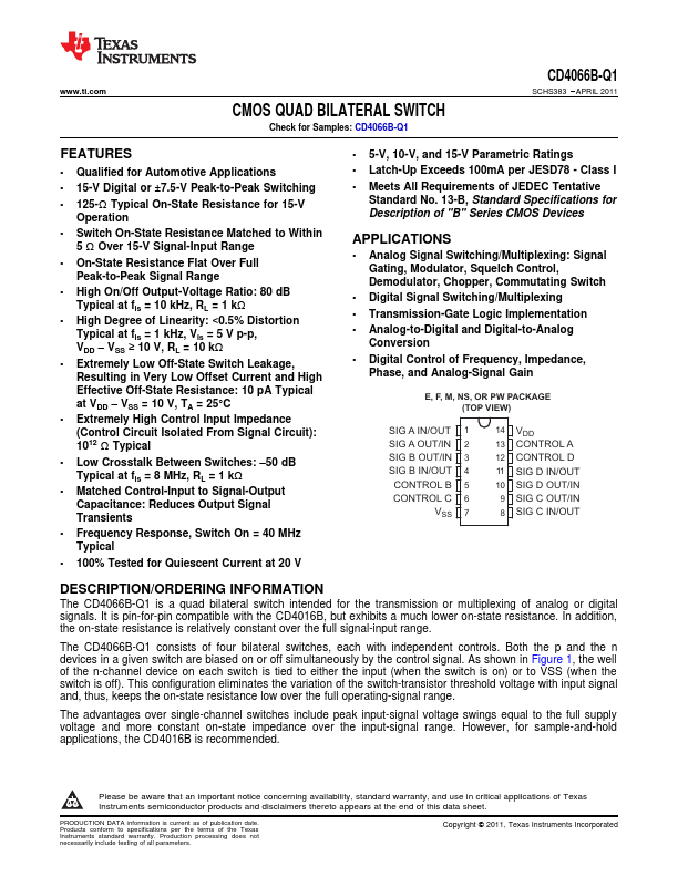
CD4066B-Q1
SCHS383
- APRIL 2011
Features
- Qualified for Automotive Applications
- 15-V Digital or ±7.5-V Peak-to-Peak Switching
- 125-Ω Typical On-State Resistance for 15-V Operation
- Switch On-State Resistance Matched to Within 5 Ω Over 15-V Signal-Input Range
- On-State Resistance Flat Over Full Peak-to-Peak Signal Range
- High On/Off Output-Voltage Ratio: 80 dB Typical at fis = 10 kHz, RL = 1 kΩ
- High Degree of Linearity: <0.5% Distortion Typical at fis = 1 kHz, Vis = 5 V p-p, VDD
- VSS ≥ 10 V, RL = 10 kΩ
- Extremely Low Off-State Switch Leakage, Resulting in Very Low Offset Current and High Effective Off-State...