Datasheet4U Logo Datasheet4U.com

CD54HCT367 - Three-State Non-Inverting and Inverting

Download the CD54HCT367 datasheet PDF. This datasheet also covers the CD54HC367 variant, as both devices belong to the same three-state non-inverting and inverting family and are provided as variant models within a single manufacturer datasheet.

General Description

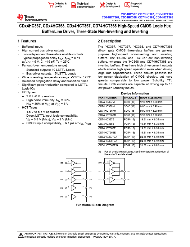
The ’HC367, ’HCT367, ’HC368, and CD74HCT368 silicon gate CMOS three-state buffers are general purpose high-speed non-inverting and inverting buffers.

The ’HC367 and ’HCT367 are non-inverting buffers, whereas the ’HC368 and CD74HCT368 are inverting buffers.

Key Features

  • Buffered inputs.
  • High current bus driver outputs.
  • Two independent three-state enable controls.
  • Typical propagation delay tPLH, tPHL = 8 ns at VCC = 5 V, CL =15 pF, TA = 25℃.
  • Fanout (over temperature range).
  • Standard outputs: 10 LSTTL Loads.
  • Bus driver outputs: 15 LSTTL Loads.
  • Wide operating temperature range: -55℃ to 125℃.
  • Balanced propagation delay and transition times.
  • Significant power reduction compare.

📥 Download Datasheet

Note: The manufacturer provides a single datasheet file (CD54HC367-etcTI.pdf) that lists specifications for multiple related part numbers.

Full PDF Text Transcription for CD54HCT367 (Reference)

Note: Below is a high-fidelity text extraction (approx. 800 characters) for CD54HCT367. For precise diagrams, and layout, please refer to the original PDF.

CD54HC367, CD74HC367, CD54HCT367 CD74HCT367, CD54HC368, CD74HC368, CD74HCT368 SCHS181E – NOVEMBER 1997 – REVISED FEBRUARY 2022 CDx4HC367, CDx4HC368, CDx4HCT367, CD74HCT36...

View more extracted text
97 – REVISED FEBRUARY 2022 CDx4HC367, CDx4HC368, CDx4HCT367, CD74HCT368 High-Speed CMOS Logic Hex Buffer/Line Driver, Three-State Non-Inverting and Inverting 1 Features • Buffered inputs • High current bus driver outputs • Two independent three-state enable controls • Typical propagation delay tPLH, tPHL = 8 ns at VCC = 5 V, CL =15 pF, TA = 25℃ • Fanout (over temperature range) – Standard outputs: 10 LSTTL Loads – Bus driver outputs: 15 LSTTL Loads • Wide operating temperature range: -55℃ to 125℃ • Balanced propagation delay and transition times • Significant power reduction compared to LSTTL Logic ICs • HC Types – 2 V to