CD74HC14PW
Description
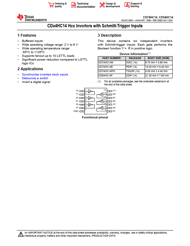
This device contains six independent inverters with Schmitt-trigger inputs.
Key Features
- Buffered inputs
- Wide operating voltage range: 2 V to 6 V
- Wide operating temperature range
- 55°C to +125°C
- Supports fanout up to 10 LSTTL loads
- Significant power reduction pared to LSTTL
Applications
- Synchronize inverted clock inputs