CD74HC365-Q1
Description
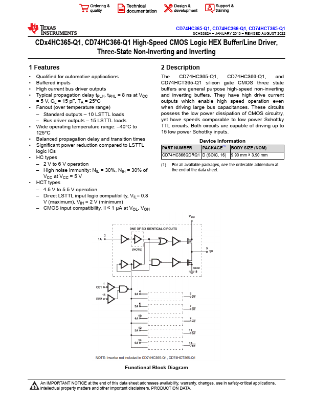
The CD74HC365-Q1, CD74HC366-Q1, and CD74HCT365-Q1 silicon gate CMOS three state buffers are general purpose high-speed non-inverting and inverting buffers. They have high drive current outputs which enable high speed operation even when driving large bus capacitances.
Key Features
- Qualified for automotive applications
- Buffered inputs
- High current bus driver outputs
- Typical propagation delay tPLH, tPHL = 8 ns at VCC = 5 V, CL = 15 pF, TA = 25°C
- Fanout (over temperature range) - Standard outputs - 10 LSTTL loads - Bus driver outputs - 15 LSTTL loads
- Wide operating temperature range: -40°C to 125°C
- Balanced propagation delay and transition times
- Significant power reduction compared to LSTTL logic ICs
- HC types - 2 V to 6 V operation - High noise immunity: NIL = 30%, NIH = 30% of VCC at VCC = 5 V
- HCT types - 4.5 V to 5.5 V operation - Direct LSTTL input logic compatibility, VIL= 0.8 V (maximum), VIH = 2 V (minimum) - CMOS input compatibility, Il ≤ 1 μA at VOL, VOH