Texas Instruments CD74HC4094E
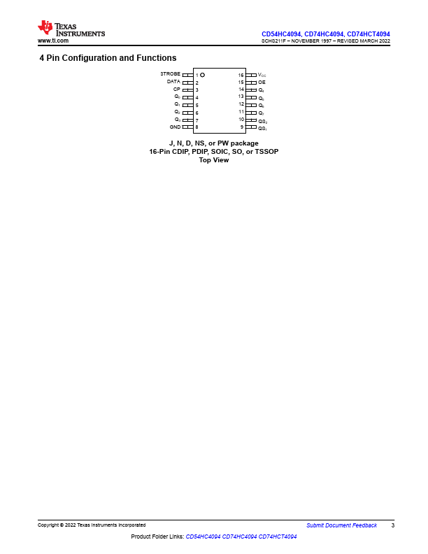
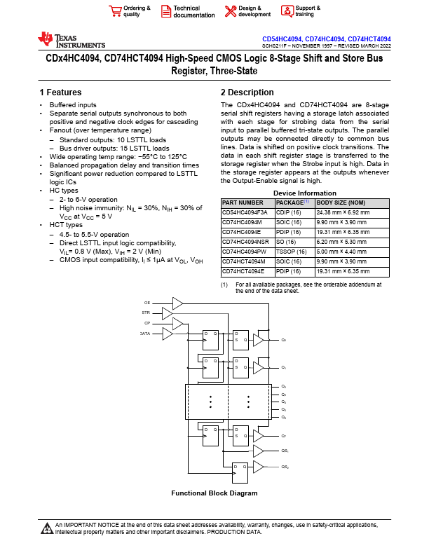
The CDx4HC4094 and CD74HCT4094 are 8-stage serial shift registers having a storage latch associated with each stage for strobing data from the serial input to parallel buffered tri-state outputs. The parallel outputs may be connected directly to common bus lines.CD74HC4094E Specifications
- Package : PDIP
- Mount Type : Through Hole
- Min Voltage : 2V
- Max Voltage : 6V
- Quiescent Current : 8µA
- Bits : 8
- Frequency : 60MHz
- Circuits : 2
- Propagation Delay : 295ns
- Logic Function : AND, Latch, Shift Register
- Max Operating Temp : 125°C
- Min Operating Temp : -55°C
Source:
Octopart
| Part No. | CD74HC4094E |
|---|---|
| Datasheet | CD74HC4094E Download |
| Manufacturer |  Texas Instruments |
| Description | 8-Stage Shift and Store Bus Register |
| Buy | Stock & Price |
FEATURES
● Buffered inputs● Separate serial outputs synchronous to both positive and negative clock edges for cascading
● Fanout (over temperature range) – Standard outputs: 10 LSTTL loads – Bus driver outputs: 15 LSTTL loads
● Wide operating temp range: −55°C to 125°C
● Balanced propagation delay and transition times
● Significant power reduction compared to LSTTL logic ICs
● HC types – 2- to 6-V operation – High noise immunity: NIL = 30%, NIH = 30% of VCC at VCC = 5 V
● HCT types – 4.5- to 5.5-V operation – Direct LSTTL input logic compatibility, VIL= 0.8 V (Max), VIH = 2 V (Min) – CMOS input compatibility, Il ≤ 1μA at VOL, VOH 2
DESCRIPTION
Data is shifted on positive clock transitions. The data in each shift register stage is transferred to the storage register when the Strobe input is high. Data in the storage register appears at the outputs whenever the Output-Enable signal is high. PART NUMBER Device Information PACKAGE(1) BODY SIZE (NOM) CD54HC4094F3A CDIP (16) 24.38 mm × 6.92...