CD74HC4094PW
Description
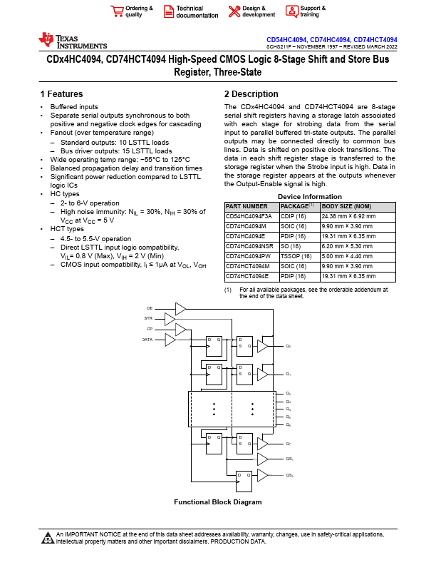
The CDx4HC4094 and CD74HCT4094 are 8-stage serial shift registers having a storage latch associated with each stage for strobing data from the serial input to parallel buffered tri-state outputs. The parallel outputs may be connected directly to common bus lines.
Key Features
- Buffered inputs
- Separate serial outputs synchronous to both positive and negative clock edges for cascading
- Fanout (over temperature range) - Standard outputs: 10 LSTTL loads - Bus driver outputs: 15 LSTTL loads
- Wide operating temp range: -55°C to 125°C
- Balanced propagation delay and transition times
- Significant power reduction compared to LSTTL logic ICs
- HC types - 2- to 6-V operation - High noise immunity: NIL = 30%, NIH = 30% of VCC at VCC = 5 V
- HCT types - 4.5- to 5.5-V operation - Direct LSTTL input logic compatibility, VIL= 0.8 V (Max), VIH = 2 V (Min) - CMOS input compatibility, Il ≤ 1μA at VOL, VOH